Difference between revisions of "TamarD Logbook"
| Line 1,923: | Line 1,923: | ||
[http://www.fnal.gov/projects/ckm/jlab/726-spec.htm] | [http://www.fnal.gov/projects/ckm/jlab/726-spec.htm] | ||
| + | |||
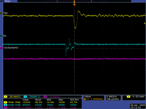
| + | <math>(15 ns(TDC Measurement) + 5 ns (PMT1 cable delay)) - ( 10 ns (ribbon cable going to TDC Stop(PMT2)) + 5 ns (Level Translator Model 726 for PMT2(stop))) = 5 ns (between the PMT1 and PMT2 pulses due to distance)</math> | ||
| + | |||
[[Delta_D_over_D]] | [[Delta_D_over_D]] | ||
Revision as of 20:02, 6 January 2010
9/5/08
Detector Construction
4 chambers are built.
TGEM:
Foils have been mounted on the TGEM comparison chamber. Both charge collectors are mounted on the TGEM test detectors. One TGEM test detector has the Thick PC board GEM foils which need much higher HV than the regular GEM foils. The second TGEM test chamber has 3 GEM foils from CERN.
Need a min of 32 1 Meg Ohm resistors to complete the output termination connectors. Need 32 more termination connectors made from 16 wires.
Need to grind down 16, M3 bolts for mounting the GEM foils and TGEM PCboards.
Need 24 washers for GEM foils. Check mounting of the TGEM boards. Look up spacing and HV for the TGEM boards[1], Media:01352098.pdf .
Need to etch 2 cathodes for the TGEm boards.
Qweak:
a.) Need to do final outer footprint machining so there is no interference with the Electron profile of the other octant.
b.) Need to machining back of the chamber for the Charge collector
c.) Need to machine thick frames for the cathode and maybe GEM foils.
d.) Apply electrical insulation to HV distribution boards
e.) Need to mount GEM foils on the Qweak chambers.
SIS3610 I/O software
Objectives: a.) The first step will be to read 16 of the I/O input channel into a CODA data file.
b.) Display the 16 input channels on a GUI. Unfortunately, only 2 of the 16 will be used to read in the GEM output. The GEM output will transfer 128 hit/no hit signals to a single I/O channel in a serial fashion. The data from one I/O channel needs to be decoded according to the data structure described in Figure 8 and 9 of the VFAT manual.
c.) The final task will be to write a multiple trigger function so the I/O can be triggered by several different interrupt trigger signals and label those trigger signals.
Tasks:
Inject a signal into the I/O board input connector and use a Read function from the ROC to determine if the signal is high or low.
9/19/08
Detector work
TGEM assembled and ready for testing.
Need to assemble GEM comparison detector.
Made 2 thick frames for Qweak Cathode.
Get Fe source from TSO on loan for many months.(done)
Machine hole punch for Qweak charge collector holes(done)
Drill holes in Qweak chamber for Charge collector mounting
Measure sag of Qweak foils and cathode. Try using a string stretched across the frame
SIS3610 I/O software
Tasks:
Inject a signal into the I/O board input connector and use a Read function from the ROC to determine if the signal is high or low.
The SIS module latches input when a VME read is initiated
The command below sets a low constant output level on the SIS output which is then conencted to one of the SIS input line directly.
-> s3610WriteOutput(0,12288)
value = 0 = 0x0
I initiated a read function and saw the following bits set
-> s3610ReadInput(0)
value = 18464 = 0x4820
Now I zero the output and read call the read function
-> s3610WriteOutput(0,0)
value = 0 = 0x0
-> s3610ReadInput(0)
value = 2080 = 0x820
I am clearly turning bits on and off but there is some randomness to other channels. Perhaps terminationg the other channels in 100 Ohms will solve this problem.
Check
created subroutine in SIS3610 library to generate a single pulse according to an given bit pattern passed as a decimal number
void TDpulse(int id, unsigned int val) {
 if((id<0) || (s3610p[id] == NULL)) {
   logMsg("s3610WriteOutput: ERROR : SIS3610 id %d not initialized \n",id,0,0,0,0,0);
   return;
 }
 s3610p[id]->d_out = val;
 s3610p[id]->d_out = 0;
 return;
}
-> TDpulse(0,12288) value = 0 = 0x0
Now we tried to use
-> TDpulse(0,12288) value = 0 = 0x0 -> s3610ReadInput(0) value = 2080 = 0x820
2080 d = 100011000 b => channel 4,5 and 9 were high
The input did not change
I think we need to Latch it.
18464 d = 100100000100000 b
Read manual to see how to latch the input.
9/26/08
Detector Construction
Both GEM and TGEM proto type detectors have been assembled.
TGEM draws 200 A at 800 Volts Need to see why.
Ramp voltage at 1 V/sec. Saw discharges on scope when increasing HV at rate of 5 V/s.
Ramping up the voltage on TGEM and GEM at 2 V/sec.
| GEM Drift HV (Volts) | GEM Drift current A | GEM foil HV (Volts) | GEM foil current A |
| 3800 | 0 | 3500 | 845 |
GEM Detector HV settings and Pulses
| GEM Drift HV (Volts) | GEM Drift current A | GEM foil HV (Volts) | GEM foil current A | Scope Picture |
| 3950 | 3650 | 882 | 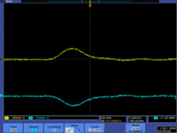
| |
| 3900 | 3600 | 870 | 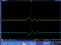
| |
| 3850 | 3550 | 859 | 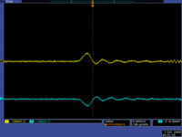
|
| TGEM Drift HV (Volts) | TGEM Drift current A | TGEM foil HV (Volts) | TGEM foil current A |
| 3600 | 3300 |
SIS310
1.) Get 100 Ohm resistors
2.) Get Bread board
10/3/08
The high current draw (> 1mA) of the TGEM on the power supply has forced us to switch to powering each PCboard GEM individually. We now have 4 HV channels hooked up with the ground floating on the top 2 GEM PCboards.
GEM Detector
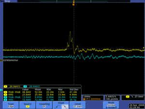
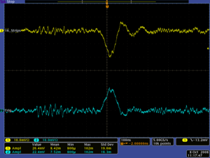
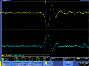
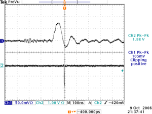
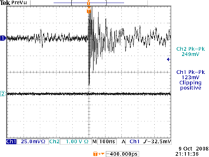
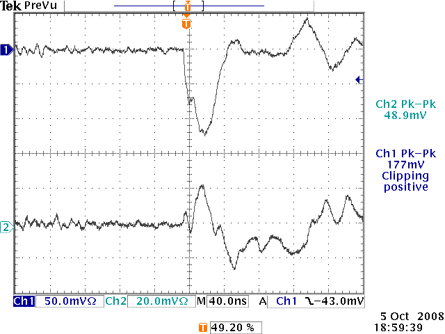
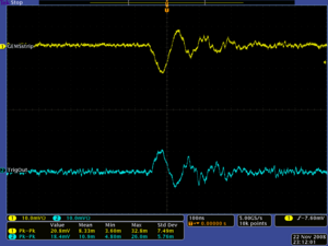
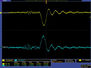
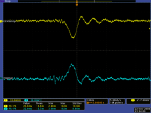
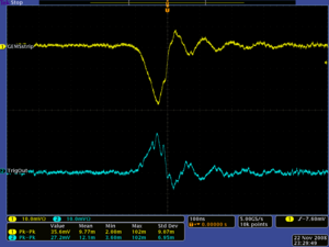
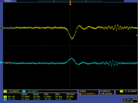
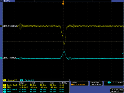
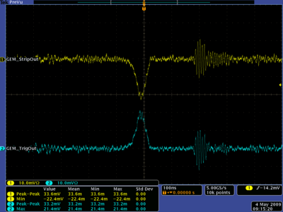
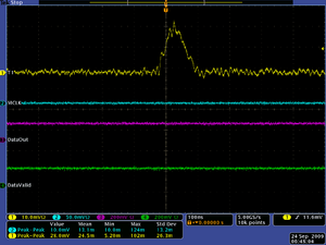
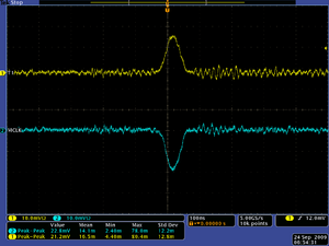
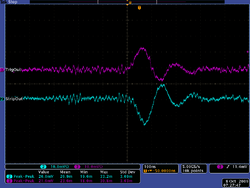
Vdrift = 3800, VGem = 3500, IDrift = 0, IGem = 842 A. Channel 1 is the output of 16 strips tied together. The remaining output strips have a 1 M Ohm resister to ground. Channel 2 is the Trigger output (the output from the last foil). Notice the sign difference between the 2 outputs.
Vdrift = 3850, VGem = 3550, IDrift = 0, IGem = 858 A
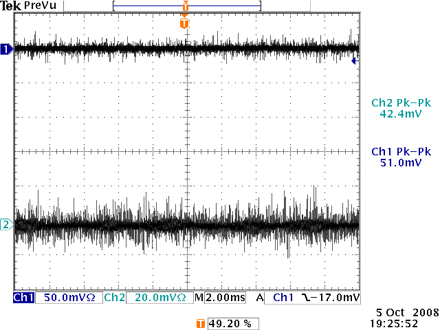
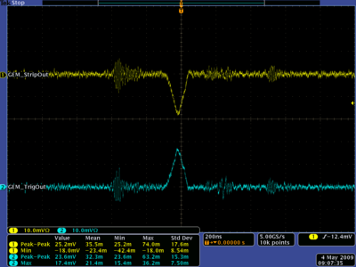
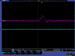
Output from the GEM detector strips and from TrigOut after signal goes through the Timing Filter Amp(amplifier was set to "x10").
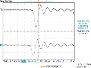
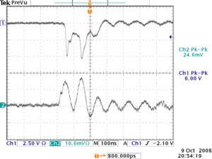
The output from GEM detector strips and TrigOut(after it goes through electronics):
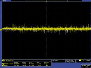
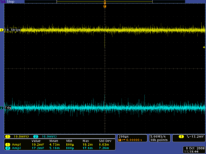
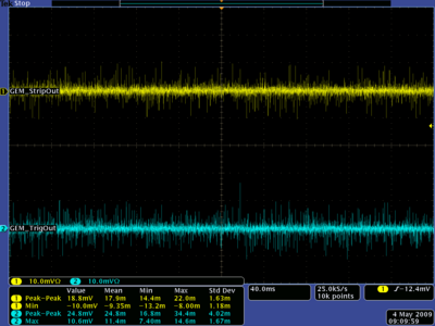
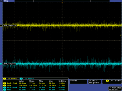
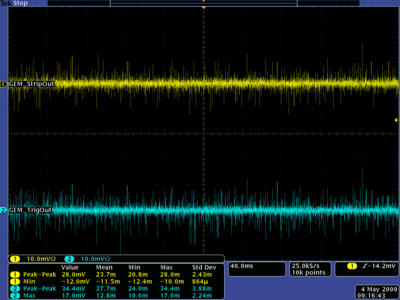
Noise level will be documented.
The GEM detector is working!
GEM DETECTOR IS READY WITH ELECTRONICS
THGEM Detector
Lets check the TGEM detector
Media:TheTHGEM_MasterThesis_Chen_Ken_Shalem.pdf
The distance between the THGEM foils is 2 mm(before it was ~1.5 mm) and the distance between the last THGEM foil and cathode is about ~5 mm. I have not changed the distance between the PCB(Charge collector) and the first THGEM foil.(might do it)
THGEM detector is not working still at high voltages.
For now HVSettings are following(I still have sparks, but they are very few, and I think they come from THGEM foils)
HVsettings
| Cathode HV (Volts) | First THGEM foil(Volts) | Second THGEM foil(Volts) | Third THGEM foil(Volts) | Third THGEM foil current A |
| 3000 | 1650 | 1500 | 1500 | 1181 |
11/21/08
a.)ship out Qweak GEM
Rectangular GEM detector works after replacing all 3 GEM preamp foils!!!!!!!!
Need to replace foils one at a time to see which one is bad and then determine why it is bad. Short?
Distance between the GEM foils are 2 mm. Distance between the last GEM foil and PCB is also 2 mm. The first GEM foil and cathode are separated by 3 mm.
Ramp Up = 2 Volts/sec.
Can go up to Volts without even one spark and Volts.
11-25-08
1.) One GEM foil is bad.
2.) Second GEM foil works:
High Voltage on Drift was 3800Volts and on GEM 3500 Volts.
3.) Third GEM foil works:
High Voltage on Drift was 3800Volts and on GEM 3500 Volts(Sparks).
I see spots on the above "working" GEM foils.  Let's leave them out and keep the three new ones in.

DONE
Why is the "1" GEM foil not working?
Do not know yet.
Testing DC
HV Settings:
| HV settings | ||
| Wire | Volts | |
| Sense | 1700 | |
| Field | -850 | |
| Guard | 850 | |
Gas type: ArCO2 (90/10).
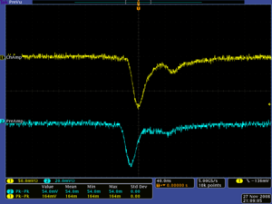
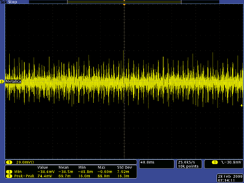
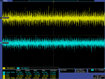
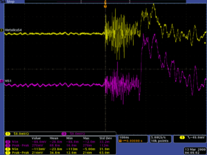
Below are shown the scope images of the signal from the DC(direct output from the sense wires):
Metalica
Plastika
Need UVA 122B Signal Splitter
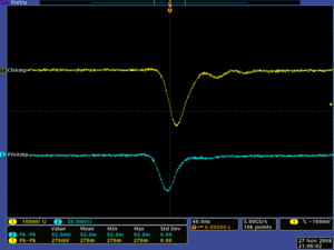
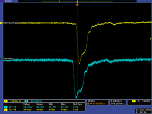
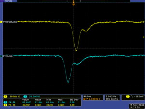
PreAmp should be set to 6.5 Volts, otherwise we get the ring(noise level is high).
PreAmp, Chamber Amp && VPIPostAmp
Gas type: ArCO2 (90/10).
The voltage on PreAmp is set to 6.5 Volts.
HV Settings:
| HV settings | ||
| Wire | Volts | |
| Sense | 1500 | |
| Field | -750 | |
| Guard | 750 | |
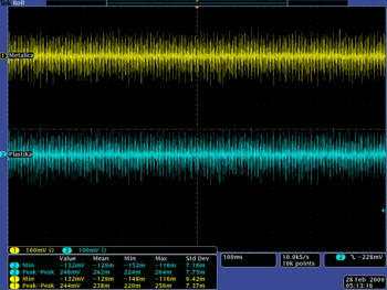
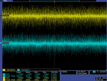
The signal outputs from the PreAmp and ChamberAmp compared for Metalica && Plastika.
The signal outputs and noise level from the PreAmp and VPIPostAmp(TDC output) compared for Metalica && Plastika.
GEM 29-11-08
The strip output signal is used as a trigger and as a pulse too.
Gas type ArCO2 (90/10).
HV Settings: Volts and Volts.
Data: r564 and r571.
CAEN V775 TDC
From the results shown below one can make conclusions that the time interval between the end of the pulses effects the data.
The table below shows the TDC measurement made using the Stanford pulse generator to generate 2 ECL input pulses. The first pulse is defined to rise at point "A" in time and fall at point "B" in time. The second pulse rises at point "C" in time and falls at point "B" in time. Comparing the time intervals between the pulses to the TDC output indicates that the TDC measures the time interval BD.
| A | B | C | D | TDC | AC | AD | BC | BD |
| 0 | 60 | 150 | 200 | 2526 | 150 | 200 | 90 | 140 |
| 0 | 90 | 150 | 200 | 1942 | 150 | 200 | 60 | 110 |
| 0 | 90 | 150 | 230 | 2504 | 150 | 230 | 60 | 140 |
| 30 | 60 | 150 | 200 | 1927 | 120 | 170 | 90 | 140 |
| 30 | 60 | 130 | 200 | 2501 | 100 | 170 | 70 | 140 |
First case
A=T+0
B=A+60ns
C=T+150ns
D=T+200ns
-> c775Reset
value = 0 = 0x0
-> c775Status(0)
STATUS for TDC id 0 at base address 0x90610000
----------------------------------------------
Interrupts Disabled
Last Interrupt Count    : 0
            --1--  --2--
 S-> c775Reset
value = 0 = 0x0
-> c775Status(0)
STATUS for TDC id 0 at base address 0x90610000
----------------------------------------------
 Interrupts Disabled
 Last Interrupt Count    : 0
            --1--  --2--
  Status  = 0x0053 0x0000  (Data Ready)
  BitSet  = 0x0000 0x4880
  Control = 0x0000
  FSR     = 440 nsec
  Event Count     = 1
  Last Event Read = (No Events Read)
 value = 37 = 0x25 = '%'
-> c775PrintEvent
 TDC DATA for Module 0
 Header: 0xfa000100   nWords = 1
     0xf80249de
 Trailer: 0xfc000000   Event Count = 0
value = 3 = 0x3
->
TDC bits 100111011110 b = 2526 d
Second case
A=T+0
B=A+90ns
C=T+150ns
D=T+200ns
-> c775PrintEvent
 TDC DATA for Module 0
 Header: 0xfa000100   nWords = 1
     0xf8024796
 Trailer: 0xfc000003   Event Count = 3
value = 3 = 0x3
-> c775Status(0)
STATUS for TDC id 0 at base address 0x90610000
----------------------------------------------
Interrupts Disabled
Last Interrupt Count    : 0
            --1--  --2--
 Status  = 0x005f 0x0004  (Buffer Full)
 BitSet  = 0x0000 0x4880
 Control = 0x0000
 FSR     = 440 nsec
 Event Count     = 217
 Last Event Read = 3
value = 22 = 0x16
->
The TDC Bits 011110010110 b = 1942 d
Third case
A=T+0
B=A+90ns
C=T+150ns
D=T+230ns
-> c775Status(0)
STATUS for TDC id 0 at base address 0x90610000
----------------------------------------------
Interrupts Disabled
Last Interrupt Count    : 0
            --1--  --2--
 Status  = 0x0053 0x0000  (Data Ready)
 BitSet  = 0x0000 0x4880
 Control = 0x0000
 FSR     = 440 nsec
 Event Count     = 5
 Last Event Read = (No Events Read)
value = 37 = 0x25 = '%'
-> c775PrintEvent
 TDC DATA for Module 0
 Header: 0xfa000100   nWords = 1
     0xf80249c8
 Trailer: 0xfc000000   Event Count = 0
value = 3 = 0x3
->
TDC bits 100111001000 b = 2504 d
Fourth case
A=T+30ns
B=A+60ns
C=T+150ns
D=T+200ns
-> c775Status(0)
STATUS for TDC id 0 at base address 0x90610000
----------------------------------------------
Interrupts Disabled
Last Interrupt Count    : 0
            --1--  --2--
 Status  = 0x0053 0x0000  (Data Ready)
 BitSet  = 0x0000 0x4880
 Control = 0x0000
 FSR     = 440 nsec
 Event Count     = 5
 Last Event Read = (No Events Read)
value = 37 = 0x25 = '%'
-> c775PrintEvent
 TDC DATA for Module 0
 Header: 0xfa000100   nWords = 1
     0xf8014787
 Trailer: 0xfc000003   Event Count = 3
value = 3 = 0x3
->
TDC : 011110000111 b = 1927 d
Fifth case
A=T+30ns
B=A+60ns
C=T+130ns
D=T+200ns
-> c775Status(0)
STATUS for TDC id 0 at base address 0x90610000
----------------------------------------------
Interrupts Disabled
Last Interrupt Count    : 0
            --1--  --2--
 Status  = 0x0053 0x0000  (Data Ready)
 BitSet  = 0x0000 0x4880
 Control = 0x0000
 FSR     = 440 nsec
 Event Count     = 3
 Last Event Read = 0
value = 22 = 0x16
-> c775PrintEvent
 TDC DATA for Module 0
 Header: 0xfa000100   nWords = 1
     0xf80149c5
 Trailer: 0xfc000000   Event Count = 0
value = 3 = 0x3
->
TDC bits 100111000101 b = 2501 d
TDC AND DC
-> c775PrintEvent
 TDC DATA for Module 0
 Header: 0xfa000200   nWords = 2
     0xf80040e8  0xf80f415f
  Trailer: 0xfc000004   Event Count = 4
value = 4 = 0x4
Checking PMT
-> c775PrintEvent
 TDC DATA for Module 0
 Header: 0xfa001000   nWords = 16
     0xf8004252  0xf80140e9  0xf80240d3  0xf80340e5  0xf80440e5
     0xf80540f4  0xf80640ef  0xf807418a  0xf8084195  0xf80942d9
     0xf80a418b  0xf80b4184  0xf80c4140  0xf80d413d  0xf80e4152
     0xf80f414d
 Trailer: 0xfc000000   Event Count = 0
value = 18 = 0x12
-> c775PrintEvent
 TDC DATA for Module 0
 Header: 0xfa001000   nWords = 16
     0xf8004214  0xf8014172  0xf802415a  0xf80340af  0xf804416e
     0xf805417a  0xf806424a  0xf80740b5  0xf80841a5  0xf809419a
     0xf80a40b9  0xf80b4195  0xf80c418e  0xf80d40b2  0xf80e4193
     0xf80f4184
 Trailer: 0xfc000001   Event Count = 1
value = 18 = 0x12
1/29/09
Checking TDC
| Sense Wire | Run Number |
| # 1 | r722 |
| #2 | r723 |
1/30/09
1.) decrease DC HV well below 1000 Volts
2.) unplug postamp outputs and do a channel by channel test of DAQ DC ADC and TDC readout
3.) calculate gas consumption rate Liters/hr
The Volume of 1 mole of an Ideal gas
24.47 litres (24.47L) at S.L.C
[Standard Laboratory Conditions, 25oC (298K) and 101.3kPa (1atm)]
Amount of ArCO2 in Liters
4.)Develop apparatus to measure gas chamber leaks.
File:Chamber leak rate measurement 2002 03 13.pdf
5.) Enter Calorimeter cuts used for electron and pion cuts into wiki and put link to them in the Teleconference wiki area
6.) Prepare next items for EG1 teleconference : E/P graphs for electron and pions before and after cuts, try to use all of the data we use for asymemtries. Also put in table estimating number of events we expect after cuts.
2/6/09
1.) Plateau DC using singles counting
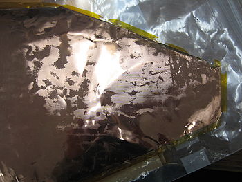
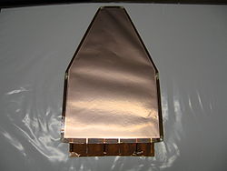
2.) Take picture of chamber and upload into wiki, Prep Qweak chamber for testing
shopping list for Norco: Gas flow valve, copper lines, shutoff valve, something to go from copper line to quick connect on Qweak chamber (compression fitting.
3.) write up procedure and part list to leak test CLAS12 R1 drift chambers
4.) pions
NPE -vs- EC/p for e- with cuts?
5.) Estimate of pion contamination
6.) difference W-spectrum for each run number add link to wiki location for teleconference.
7.) recheck the sign of all polarization for plots of semi-inclusive spectrum: a.) h>0 Pt>0 b.) h > 0 pt<0 c.)h<0 pt>0 d.)h<0 pt<0
2-06-09
Checking TDC Outputs
Real Signal From DCs
Using Drift Chambers
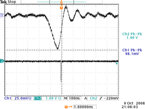
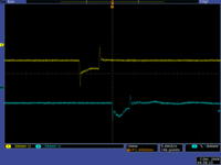
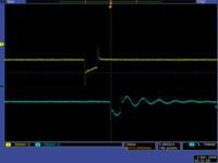
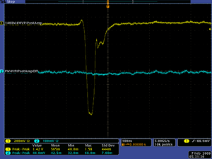
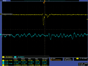
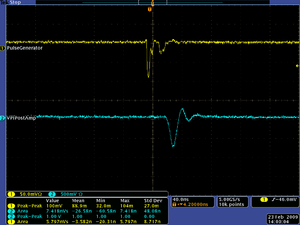
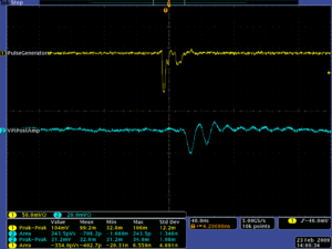
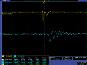
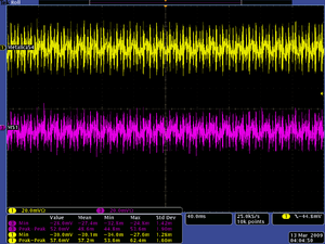
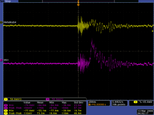
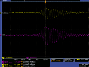
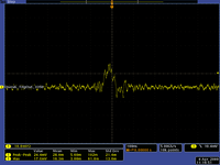
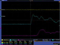
The scope images below describe the crosstalk which exists in the UVA splitter and the VPI postamp. For both DCs only Sense Wire 4 is used. The high voltage on Plastika is turned Off and Metalica's HV is set to (1425:-700:990). The PreAmp is set to 6.4 Volts and hooked up on both detectors. We are able to minimize the cross talk by maximizing the distance between the connector pins used to transport the sense wire #4 signal from the 2 DC to the DAQ.
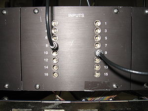
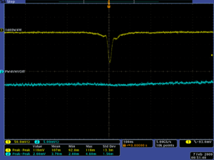
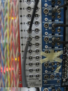
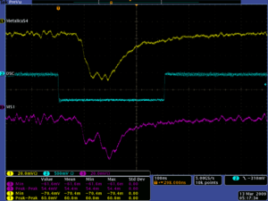
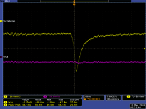
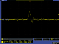
The output signal from the DCs after PreAmp are sent to the UVA 122B Signal Splitter on channel # 8 an 9 for Metalica and Plastika respectevily. The scope image below shows that approximately 1/30 of Metalicas output signal appears on Plastika's channel, as a result of the two channels being next to each other.
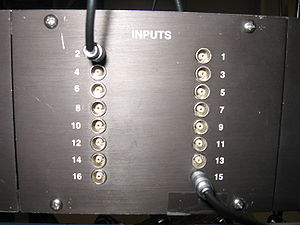
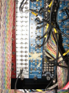
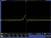
In order to decrease interference from occupying nearby channels in the UVA 122B signal splitter, the pulse output from the detectors are sent to the channel number 2 for Metalica and channel # 15 for Plastika. The cross talk caused by the UVA 122B signal splitter is far less then in first case, which was described above.
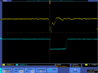
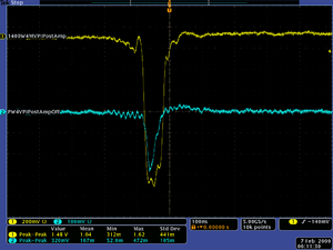
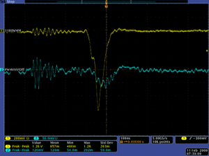
The output signals from the UVA 122B signal splitter from channels 8 and 9 of Metlica and Plastika are sent through channels 10 and 9 of the VPI post amp. 1/4 of the signal from Metalica appears on channel 9, which is TDC output for Plastika. This kind of signal, which actually comes from the Metalica, can be misidentified as a real pulse from the Plastika.
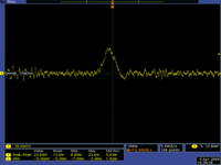
Sense wire # 4 for Metalica and Plastika from the UVA 122B signa splitter channel numbers 2 and 15 are sent to the VPI post amp channels 16 and 3. One can see on the scope picture that the cross talk between the two detectors decreased considerably.
|
||
|
Using The Stanford Pulse Generator
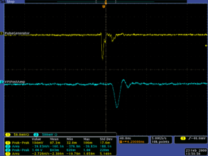
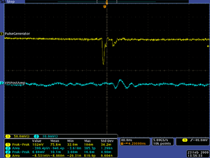
The Stanford Pulse Generator output pulse is going through the VPI PostAmp without using the UVA 122B Signal Splitter. The gain on the VPI PostAmp is set to maximum. Three channel outputs are observed on the scope. The signal is connected to channel # 15 on VPI PostAmp(the first scope image in the tabla below). The neighboring channels 14 and 16 are also shown below.
- Gain settings
- Channel # 14 - X3; channel # 15 - X10; channel # 16 - x10.
The generated signal from the Stanford Pulse Generator is sent through the UVA 122B Signal Splitter and than is connected to the VPI PostAmp channel # 15. Below scope images show the cross-talk caused by using the UVA 122B signal splitter. When the gain of the neighboring ch #(14) is set to X3 1/50 of the signal appears on it, in other case when it is set to X10 - 1/10 of the pulse appears on the channel(16) output
- CONCLUSION
In order to run DCs without having the cross-talk problem we should not use the UVA 122B Signal Splitter.
Noise Problem on DCs
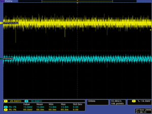
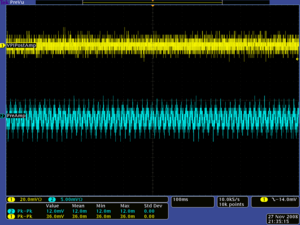
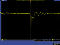
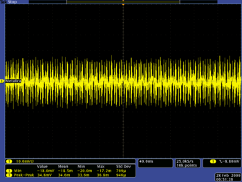
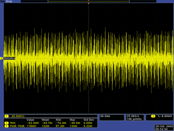
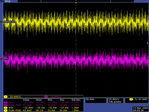
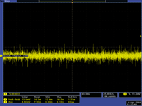
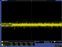
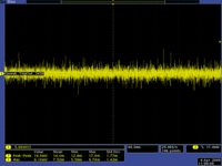
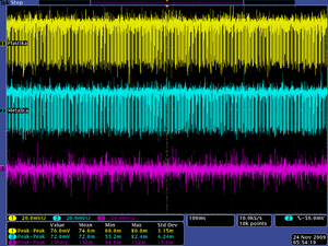
The output from DCs goes through the UVA 122B Signal Splitter and after is connected to the VPI PostAmp. The noise level for both chambers is measured and shown below on scope pictures before and after change using the grounded strip.
In this case, the output from the Metalica is connected directly to the VPI PostAmp. The noise level for minimum and maximum gains are shown below:
After connecting the grounded strip to the PreAmp box, the noise level was reduced.
The VPI PostAmp, PreAmp box are both grounded. My noise level is "perfect":
DCs
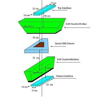
On Both chambers, Metalica and Plastika, the high voltage is applied(Settings S:F:G=1300:-650:910). The PreAmp is set to 6.4 Volts. The ArCO2(90/10) gas is flowing through the chambers. Metalika is placed between the two PMTs(only blue long PMTs are used). The cosmic coincidence event from the two PMTs is set as a trigger, ADC gate and start for the TDC.
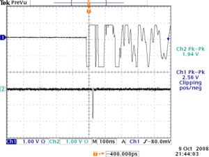
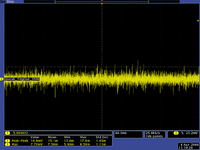
Below on the scope picture are shown two pulses, coming out from the sense wire 1(ch 3) and 4 (ch 1) after going through the VPI PostAmp in gate. Gate width on image is approximately 400 ns. I thought it was narrow so i changed it to ~ 500 ns.
1200
HV settings on Metalica S:F:G=1200:-600:840
Below is shown the noise level and typical pulse at this voltage.
1150
HV settings on Metalica S:F:G=1150:-575:805
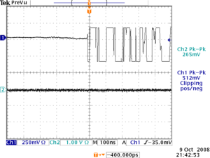
Below is shown the noise level and "pulse" caused by noise which is misidentified as a real pulse.
1100
HV settings on Metalica S:F:G=1100:-550:770
Below is shown the noise level and "pulse" caused by noise which is misidentified as a real pulse.
1.) HV Metalica 1300 Volts
Run number r751.dat
Strat: Mar 12 15:49:03
End: Mar 13 13:07:42
2.) HV Metalica 1300 Volts (only sense wire 4 in TDC)
Run number r754.dat
Strat: Mar 13 14:28:39
End: Mar 13 21:35:55
3.) HV Metalica 1300 Volts (only sense wire 4 and 1 in TDC)
Run number r755.dat
Strat: Mar 13 21:50:32
End: Mar 15 16:27:37
For 1, 2 and 3 runs discr. threshold is the same
4.) HV Metalica 1300 Volts (only sense wire 4 and 1 in TDC)
r756
Threshold doubled on Metalica
Start: mar 15 16:36:56
End: Mar 16 12:11:07
5.) HV Metalica 1200 Volts (only sense wire 4 and 1 in TDC)
r756
Threshold doubled on Metalica
Start: mar 16 12:14:30
End: Mar 17 08:30:11
5.) HV Metalica 1350 Volts
r772
Start: mar 17 13:01:27
End: Mar 17 16:47:58
5.) HV Metalica 1350 Volts (m4 and p4)
r775
Start: mar 17 19:47:57
End: Mar 18 10:38:07
Chamber Leak Rate Measurements
- List of devices needed to measure chamber leaks
- 1). The gas flow micro-calibrator (of the leak measuring device) Media:Microcalibrator_for_DC.pdf .
- 2). The Leak Measuring Device (LMD).
- 3). The Weather Monitoring Device(to measure the barometric pressure and ambient air temperature).
Using this devices, chamber leak rate is calculated in the following way:
where
- is the chamber volume
- is the change in the chamber overpressure
- is the change in the atmospheric(barometric) pressure
- is the time between the final and initial measurements of the overpressure(recommended time interval is ~ 24 hours)
- In other paper, for the chamber gas leak measurements a mass spectrometer was used
Qweak GEM Foil
Testing Qweak GEM Detector
The cathode was taken out from the chamber, and only GEM foils were tested. On GEM i went up to 3500 volts, without seeing any "sparks".
2/20/09
1.) VPI post amp cross talk measurement
Need to get rid of UVA splitter. Lets make a cable to connect 2 DC into 1 VPI input connector
2.) Do Inclusive Histograms and then do helicity difference histograms
3.) Change Qweak bottom foil, connector from Walter coming soon will use to terminate detector output
4.) Continue Plateau measurements, prepare plateau measurement run plan for April.
03-04-09
Drift Velocity Calculation
HV Settings S:F:G=1350:-675:945
Cell size d=0.86 cm
F = q E = ma
Data From DC Metalica
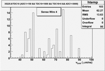
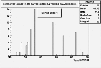
The drift velocity for electrons in drift chambers is ~ . Media:mestayer.pdf
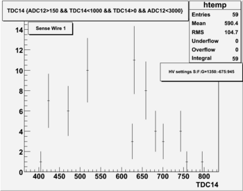
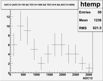
Calculated result using TDC data
The size of the drift chamber cell is 0.86 cm.
= = 61 = 6.1 cm/ s
Agrees with theoretical result.
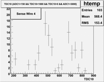
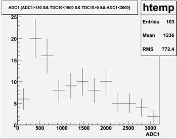
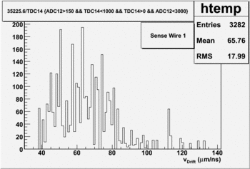
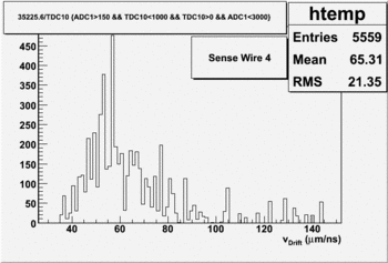
TDC and ADC measurements for Sense Wire 4
TDC and ADC measurements for Sense Wire 1
Using only bottom scintillator(TDC data)
- 1)start
- Mar 26 13:22:30
Stop: Mar 30 11:03:41
Run number r860
Only bottom Scintillator used.
- Sense Wire 1
- Sense Wire 4
SIS3610 Module
The rise of the TTL pulse into the PLX board should exceed (begin later in time) the rise SIS3610 NIM input trigger pulse in order to latch the PLX LVDS input signals sent the the SIS3610 data input connector.
- 1.)
A=T+0.000033500200
B=A-0.000033100200
C=T+0.000000333000
D=T+0.000034000000
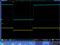
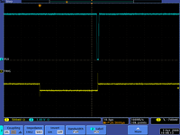
The pulse on the SIS3610 appeared after the time delay which is shown on the scope below.
2.)
A=T+0.000033500200
B=A-0.000033100200
C=T+0.000000333000
D=T+1.000034000000(one can go as high as he wants, you still have an input)
I mean increase the time interval between the pulse ends.
3.) The input data bits are not latched if the PLX rises befor the SIS3610 input TTL triger pulse
A=T+0.000033500200
B=A-0.000033100200
C=T+0.000000330000
D=T+0.000034000000
No pulse in the SIS3610 Module.
4/2/09 Qweak Detector Working
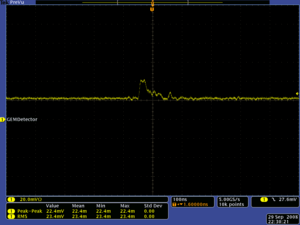
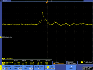
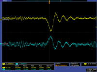
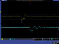
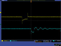
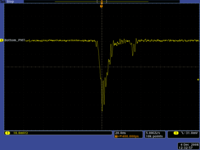
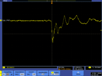
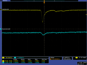
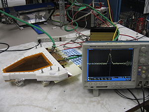
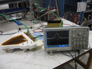
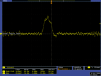
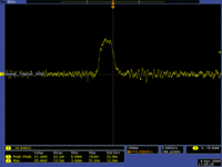
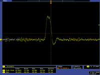
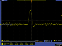
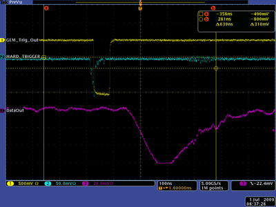
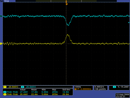
The scope pictures below shows the GEM chamber's "TrigOut" pulse caused by a cosmic ionization event in the Qweak R1 detector. The "TrigOut" pulse represents electrons leaving the last GEM preamplifier stage and is therefore a positive going pulse. The high voltage was set to -3400 Volts on the cathode and -3100 Volts on the GEM foil voltage divider network which powers all three GEM foil amplifier stages. The chamber was filled with a gas mixture composed of 90% Argon and 10% Co2 by volume. Both scope images represent the same pulses but viewed with different time scale. On the first image the time scale is set to 100 ns and on the other one - 40 ns.
Several scope pictures were taken of the trigOut pulse for different high voltages, in order to show the pulse amplitude dependence on the HV.(As the high voltage goes up, the gain of the TrigOut signal on the Qweak detector increases)
HV Drift:GEMFoil=-3300:-3000
HV Drift:GEMFoil=-3350:-3050
The trig out signal below goes away when Vdrift = VGEM=3050
HV Drift:GEMFoil=-3400:-3100
HV Drift:GEMFoil=-3450:-3150
HV Drift:GEMFoil=-3500:-3200
At 3500 Volts there are some sparks, so i didnt go on higher voltages.
| Qweak Drift/GEM HV (Volts) | Pulse amplitude | Noise level |
| 3300/3000 | 17.0 mV 4.79 mV | 6.9 mV 934 |
| 3350/3050 | 17.0 mV 12.5 mV | 6.9 mV 1.15 |
| 3400/3100 | ~20 mV 13.2 mV | 7.2 mV 886 V |
| 3450/3150 | 28.2 mV 13.0 mV | 7.52 mV 1.42 mV |
| 3500/3200 | 38.2 mV 12.4 mV | 7.7 mV 1.11 mV |
ADC Measurements For Qweak Detector
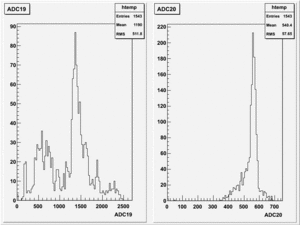
The charge from the chamber's "TrigOut" pulse was measured using a CAEN 775 charge sensing ADC. The "TrigOut" pulse was sent to an amplifier with 2 outputs. One output was sent to a discriminator to generate a trigger pulse and an ADC gate. The other output was delayed XXX ns and injected into channel YY of the CAEN ADC.
HV Settings
Electronics Settings:
HRRL 4-13-09
- 1.)
| Type of Detector | SHV Channel | BNC channel | HV Settings |
| Front Scintilator | SHV59A1 | 223A1 | -1000 Volts |
| Blue Scintilator | SHV59A2 | 223A2 | -1000 Volts |
Both scintillators were checked and they work.
05-03-09
Testing GEM Detector
HV Settings :=-3500:-3200
Not even one "spark" at this voltage.
HV Settings :=-3450:-3150
HV Settings :=-3400:-3100
Experimental SetUp
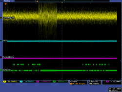
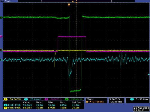
StripOut from the GEM detector is used as a gate and trigger, the signal is amplified using Timing Filter Amplifier(Model 474-09) and discriminated(DIFF CFD. Model 683). TrigOut pulse from the detector is inverted and amplified(Timing filter Amplifier Model 474-06) and delayed.
HV Drift:GEM=3450:3150
05-12-2009
Plastika(Drift Chamber) works! I am not able to get signal only from Sense wire # 4 and 5. Otherwise, all other channels are working.
06-22-2009
Media:26000Model_LogarithmicPicoammeter.pdf
Phillips Scientific 710 Octal Discriminator
- Trigger setup for GEM Detector
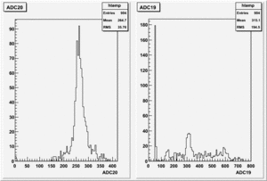
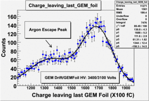
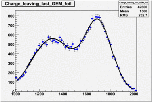
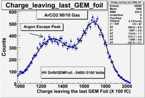
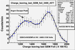
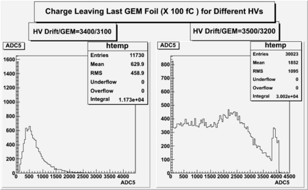
- The Histogram below shows the charge collected by the last GEM foil in Qweak detector for two HV settings
07-5-2009
DC Position Measurements Hopefully
Experimental Setup
- Beam parameters
100 ns(scope shows 200ns), 300 Hz and 40 mAmp.
- Cables and HV Settings
DC HV Settings: Sense:Field:Guard=1400:-700:980.
HV cable channels: Sense/Field/Guard=SHV59A2/A4/A3.
Signal channel - 223A9.
Pulse is amplified and after discriminated.
- PMTs
Images
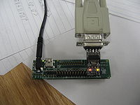
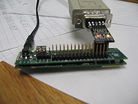
BA:53:FD:A3:7D:D1
manually set the IP:
ifconfig eth0 192.168.15.15 netmask 255.255.0.0
restart the networking (and force a retry for DHCP address:
/etc/init.d/networking restart
echo "p 32 0 0 set" | flipbit.arm
echo "p 32 0 1 set" | flipbit.arm
echo "e 32 1 6 on" | flipbit.arm
echo "e 32 134 4 on" | flipbit.arm
echo "e 32 130 0xCE set" | flipbit.arm
v1495firmware(0x80110000, "GEMReadout_Rev2-2_NoPLL.rbf",0,0)
MAC ba:53:fd:a3:7d:e1
Gumstix IP address at ISU
Compiled on Feb 21 2005, 19:32:30.
Press CTRL-A Z for help on special keys
.o��ti��o.t �ter 60 �co��.
OpenEmbedded Linux gumstix-custom-verdex ttyS0
Angstrom 2007.9-test-20080512 gumstix-custom-verdex ttyS0
gumstix-custom-verdex login:
OpenEmbedded Linux gumstix-custom-verdex ttyS0
Angstrom 2007.9-test-20080512 gumstix-custom-verdex ttyS0
gumstix-custom-verdex login: root
Password:
Welcome to gumstix!
For information on how to customize or update this software please visit:
http://www.gumstix.net
root@gumstix-custom-verdex:~$ root@gumstix-custom-verdex:~$ ls
bin        hello.arm
root@gumstix-custom-verdex:~$ /sbin/ifconfig
eth0      Link encap:Ethernet  HWaddr DE:23:D5:65:A1:10
         inet addr:134.50.3.175  Bcast:134.50.3.255  Mask:255.255.255.0
         UP BROADCAST RUNNING MULTICAST  MTU:1500  Metric:1
         RX packets:640687 errors:0 dropped:0 overruns:0 frame:0
         TX packets:3657 errors:0 dropped:0 overruns:0 carrier:0
         collisions:0 txqueuelen:1000
         RX bytes:57825718 (55.1 MiB)  TX bytes:380094 (371.1  KiB)
lo        Link encap:Local Loopback
         inet addr:127.0.0.1  Mask:255.0.0.0
         UP LOOPBACK RUNNING  MTU:16436  Metric:1
         RX packets:0 errors:0 dropped:0 overruns:0 frame:0
         TX packets:0 errors:0 dropped:0 overruns:0 carrier:0
         collisions:0 txqueuelen:0
         RX bytes:0 (0.0 B)  TX bytes:0 (0.0B)
root@gumstix-custom-verdex:~$
root@134.50.3.175
interrupt: ERROR: v1495ReadEvent returned 0 words
interrupt: ERROR: v1495ReadEvent returned 0 words
interrupt: ERROR: v1495ReadEvent returned 0 words
interrupt: ERROR: v1495ReadEvent returned 0 words
12/08/2009
The Qwaek GEM detector works. HV settings:
CODA running
17/08/2009
| Outputs | Channel Number |
| TOP PMT singles | 1 |
| Bottom PMT singles | 3 |
| Top + Bottom PMT coincidence | 5 |
| GEM Trig out singles | 7 |
| GEM Trig out + Top PMT coincidence | dont have |
| GEM Trig out + Bottom PMT coincidence | 9 |
| GEM Trigout + Top + Bottom PMT coincidence | 13 |
| Time (1 Hz) | 15 |
Used Timing Filter Amplifier(Noise level was high, and leading edge discriminator instead of CFD)
| Run # | HV=Drift/GEM Volts | TOP PMT singles (1) | Bottom PMT singles (3) | Top + Bottom PMT coincidence (5) | GEM Trig out singles (7) | GEM Trig out + Bottom PMT coincidence (9) | GEM Trigout + Top + Bottom PMT coincidence (13) | Time (1 Hz) (15) | 13/5 (%) |
| 1313 | 3520/3220 | 567251 | 1428373 | 11047 | 94075 | 520 | 146 | 79575 | 1.3 |
| 1315 | 3550/3250 | 139586 | 137090 | 997 | 1101151 | 195 | 20 | 6923 | 2.0 |
| 1316 | 3550/3250 | 896375 | 1347216 | 11098 | 79905 | 536 | 171 | 76232 | 1.5 |
| 1317 | 3575/3275 | 558724 | 875863 | 6486 | 70651 | 439 | 131 | 45558 | 2.0 |
| 1318 | 3525/3225 | 429067 | 822762 | 6419 | 38107 | 186 | 57 | 42917 | 0.9 |
| 1319 | 3600/3300 | 1445938 | 3544955 | 27578 | 440996 | 2049 | 676 | 183089 | 2.5 |
| 1320 | 3600/3300 | 618683 | 1616819 | 11867 | 192341 | 789 | 269 | 76243 | 2.3 |
Using Chamber Output Amplifier with Phillips Gain amplifier(for GEM TrigOut) and amplified is discriminated with CFD.
The GEM detector "Trig Out" signal is sent to the custom post amplifier used by the CLAS Drift chambers and then sent to an Leading Edge Discriminator. The discriminator is set to 50 mV
| Run # | HV=Drift/GEM Volts | TOP PMT singles (1) | Bottom PMT singles (3) | Top + Bottom PMT coincidence (5) | GEM Trig out singles (7) | GEM Trig out + Bottom PMT coincidence (9) | GEM Trigout + Top + Bottom PMT coincidence (13) | Time (1 Hz) (15) | 13/5 (%) |
| 1322 | 3640/3340 | 324596 | 472633 | 3059 | 25632 | 66 | 54 | 22797 |
Ethane
Ethane Properties Noncorrosive
"At room temperature, ethane is a flammable gas. When mixed with air at 3.0% – 12.5% by volume, it forms an explosive mixture." Ethane
Corrosion Resistance Tables for Ethane
Parker 7121 welding hose, Grade R
EPDM rubber (ethylene propylene diene Monomer (M-class) rubber) - Unsatisfactory.
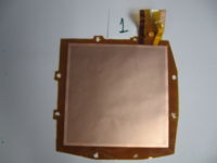
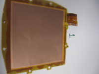
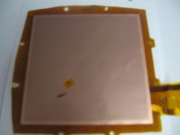
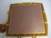
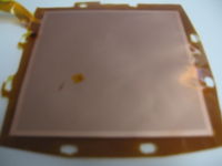
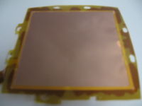
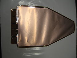
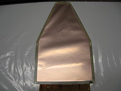
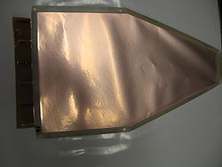
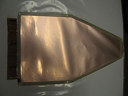
GEM Foils mounted on the frame
Media:vfat16_jlab_working_one.html
Shopping List For Dr. Forest
[3] - 10
[4] - 10
[5] - 3
[6] - 200
[7] - 200
[8] - 200
NIM BIN Modules
2 Channel 15 kV Programmable Power Supply
- Possible ones
DC efficiency
| DC HV on Sense Wire | TOP PMT singles (1) | Bottom PMT singles (3) | Top + Bottom PMT coincidence (5) | DC Singles (15) | DC + Top PMT + Bottom PMT (16) | 16/5 % |
| 1450 Volts | 675516 | 987316 | 4054 | 162777 | 202 | 4.9 |
| 1450 Volts | 1190056 | 1052420 | 4397 | 331472 | 227 |
A GEM HV of 3600/330 may give the same rate as
Baby chambers set to 1450 Volts on the sense wire.
Replacing HV board on GEM
I took apart GEM detecter and replaced the HV board.
HV Board on GEM detector is replaced and it works:
HV Settings are following:
HV Settings are following:
&&
  Scaler Data :
SCAL01:     312024  SCAL02:          0  SCAL03:    2020395  SCAL04:          0
SCAL05:       2875  SCAL06:          0  SCAL07:      40363  SCAL08:          0
SCAL09:         46  SCAL10:          0  SCAL11:          0  SCAL12:          0
SCAL13:         24  SCAL14:          0  SCAL15:     194288  SCAL16:        144
value = 0 = 0x0
&&
  Scaler Data :
SCAL01:      17984  SCAL02:          0  SCAL03:     123457  SCAL04:          0
SCAL05:        214  SCAL06:          0  SCAL07:     273805  SCAL08:          0
SCAL09:         40  SCAL10:          0  SCAL11:          0  SCAL12:          0
SCAL13:         29  SCAL14:          0  SCAL15:      14105  SCAL16:         32
value = 0 = 0x0
  Scaler Data :
SCAL01:      45510  SCAL02:          0  SCAL03:     326892  SCAL04:          0
SCAL05:        505  SCAL06:          0  SCAL07:     303950  SCAL08:          0
SCAL09:         67  SCAL10:          0  SCAL11:          0  SCAL12:          0
SCAL13:         49  SCAL14:          0  SCAL15:      38497  SCAL16:         62
value = 0 = 0x0
  Scaler Data :
SCAL01:     644627  SCAL02:          0  SCAL03:    4781886  SCAL04:          0
SCAL05:       6469  SCAL06:          0  SCAL07:    1641122  SCAL08:          0
SCAL09:        593  SCAL10:          0  SCAL11:          0  SCAL12:          0
SCAL13:        441  SCAL14:          0  SCAL15:     585088  SCAL16:        706
value = 0 = 0x0
  Scaler Data :
SCAL01:      16886  SCAL02:          0  SCAL03:     121292  SCAL04:          0
SCAL05:        183  SCAL06:          0  SCAL07:       3100  SCAL08:          0
SCAL09:         45  SCAL10:          0  SCAL11:          0  SCAL12:          0
SCAL13:         45  SCAL14:          0  SCAL15:      14959  SCAL16:         51
value = 0 = 0x0
  Scaler Data :
SCAL01:      25408  SCAL02:          0  SCAL03:     186425  SCAL04:          0
SCAL05:        320  SCAL06:          0  SCAL07:       4943  SCAL08:          0
SCAL09:        102  SCAL10:          0  SCAL11:          0  SCAL12:          0
SCAL13:        102  SCAL14:          0  SCAL15:      22765  SCAL16:        111
value = 0 = 0x0
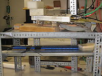
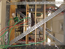
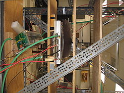
Efficiency of GEM Detector and Drift Chamber, Experimental SetUp
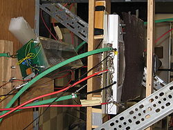 [[File:GEM_TwoPMTs_DC_28-09-09_5.jpg|250px]
Sh
- Xorg configuration created by pyxf86config
Section "ServerLayout" Identifier "Default Layout" Screen 0 "Screen0" 0 0 InputDevice "Keyboard0" "CoreKeyboard" EndSection
Section "InputDevice" Identifier "Keyboard0" Driver "kbd" Option "XkbModel" "pc105" Option "XkbLayout" "us" EndSection
Section "Device" Identifier "Videocard0" Driver "vesa" EndSection
Section "Screen" Identifier "Screen0" Device "Videocard0" DefaultDepth 24 SubSection "Display" Viewport 0 0 Depth 24 EndSubSection EndSection
Qweak_R1_A GEM Detector works
10/9/09
scal01 scal 05
  Scaler Data :
SCAL01:      37413  SCAL02:          0  SCAL03:     306915  SCAL04:          0
SCAL05:        381  SCAL06:          0  SCAL07:      15791  SCAL08:          0
SCAL09:         99  SCAL10:          0  SCAL11:          0  SCAL12:          0
SCAL13:         70  SCAL14:          0  SCAL15:     176561  SCAL16:        144
value = 0 = 0x0 -
Lab stuff
TDC Measurements
Run number: r1351.dat
Start: Nov 2, 14:13:10 Stop: Nov 16, 10:12:14
| Channel # | Detector type | TDC Histograms_1 | TDC Histograms_2 (TDC2>500) |
| 2 | Bottom Scintillator | 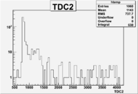 |
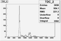
|
| 3 | Top DC(Plastika) | 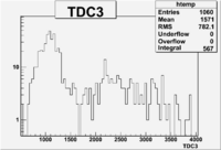 |
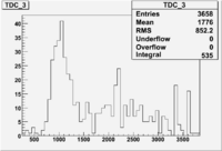
|
| 4 | Bottom DC(Metalica) | 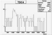 |
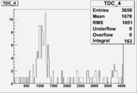
|
| 5 | Qweak GEM Detector | 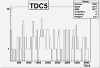 |
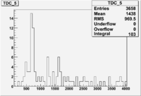
|
Electronics+TimeShift=180ns
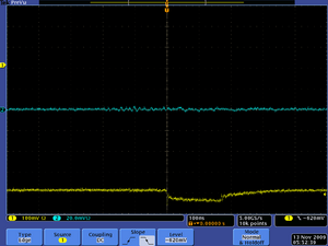
[11]
11/6/09
11/20/09
1
New TDC runs with changed Discriminator thresholds
DC-60 mV
GEM-100mV
GEM HV - 3500/3200 Volts
Run number r1353
Start: Nov 18 15:42:29
Stop: Nov 23 13:54:08
| Channel # | Detector type | TDC Histograms_1 | TDC Histograms_2 (zoomed in) |
| 2 | Bottom Scintillator | 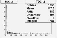 |
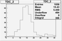
|
| 3 | Top DC(Plastika) | 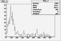 |
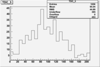
|
| 4 | Bottom DC(Metalica) | 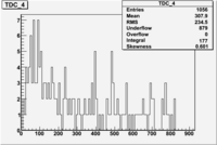 |
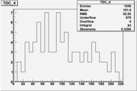
|
| 5 | Qweak GEM Detector | 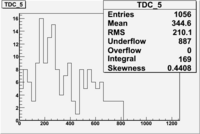 |
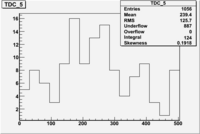
|
| Device | Peak - Peak noise (mV) |
| Plastika | 76 |
| Metalica | 72 |
| GEM 1B | 136 |
| Disciminator (mV) | Plastica Eff. (%) |
| 40 | |
| 60 | |
| 80 |
| Disciminator (mV) | Metalica Eff. (%) |
| 40 | |
| 60 | |
| 80 |
| Disciminator (mV) | GEM Eff. (%) |
| 70 | |
| 100 | |
| 140 |
The third channel is QweakGEM Detector.
2
Detectors swapped.
Run number r1356.dat
DC-60 mV
GEM-100mV
GEM HV - 3500/3200 Volts
Start: Nov 23 18:07:21
Stop: Nov 25 15:32:45
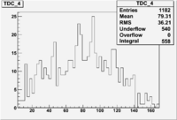
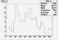
| Channel # | Detector type | TDC Histograms_1 | TDC Histograms_2 (zoomed in) |
| 2 | Bottom Scintillator | 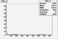 |
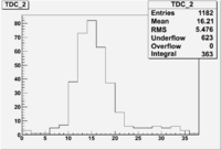
|
| 4 | Top DC(Metalica) | 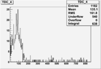 |
|
| 3 | Bottom DC(Plastika) | 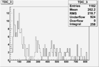 |
|
| 5 | Qweak GEM Detector | 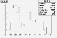 |
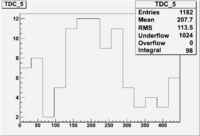
|
No cut on Bottom Scintillator
Cut on Bottom Scintillator(TDC2>500)
3
The same layout of detectors as in #2
Run number r1357.dat
DC-100 mV
GEM-140mV
GEM HV - 3500/3200 Volts
Start:
Stop:
| Channel # | Detector type | TDC Histograms_1 | TDC Histograms_2 (zoomed in) |
| 2 | Bottom Scintillator | 200px | 200px |
| 4 | Top DC(Metalica) | 200px | 200px |
| 3 | Bottom DC(Plastika) | 200px | 200px |
| 5 | Qweak GEM Detector | 200px | 200px |
shopping list for digikey && pasternack
1.) [12] - 2 per board. (order maybe 5)
and
2.) [13]
Some other items
[14]-100 feet $28
K-K 101 A004
Number of counts in PMTs
Thresholds - 34 mV
-> v260Status(0,1)
STATUS for SCALER id 0 at base address 0x90da0000
--------------------------------------------------
 Version = 0x10dc    Module Type = 0x080d
 Scalers ENABLED

  Scaler Data :
SCAL01:       7828  SCAL02:      24171  SCAL03:          0  SCAL04:      46106
SCAL05:          0  SCAL06:          0  SCAL07:          0  SCAL08:          0
SCAL09:          0  SCAL10:          0  SCAL11:          0  SCAL12:          0
SCAL13:          0  SCAL14:          0  SCAL15:          0  SCAL16:          0
value = 0 = 0x0
->
21cm, 7cm.
Both PMT's should have their gain and disc threshold set to within 25%
of the cosmic rate.  Right now the bottom PMT is not agreeing
with this request.  Either lower voltage or raise threshold.
I prefer to lower Voltage and have both PMTs on same disc. threshold setting.
After the singles rate looks good compare the coincidence rate with expectations.
  Scaler Data :
SCAL01:        714  SCAL02:        580  SCAL03:          0  SCAL04:        610
SCAL05:          0  SCAL06:          0  SCAL07:          0  SCAL08:          0
SCAL09:          0  SCAL10:          0  SCAL11:          0  SCAL12:          0
SCAL13:          0  SCAL14:          0  SCAL15:          0  SCAL16:          0
value = 0 = 0x0
->
  Scaler Data :
SCAL01:     171548  SCAL02:     136127  SCAL03:          0  SCAL04:     150097
SCAL05:          0  SCAL06:        341  SCAL07:          0  SCAL08:          0
SCAL09:          0  SCAL10:          0  SCAL11:          0  SCAL12:          0
SCAL13:          0  SCAL14:          0  SCAL15:          0  SCAL16:          0
value = 0 = 0x0
->
Identify the channels and create table of Rate with detectors identifies as Top scint or Bottom scint.
Error In Coda 2.6
12/18/09
1.) Table of cosmic data
2.) Electron efficiencies when pi+ and pi- in same scintillator but electron in 2 different scintillators. Compare inclusive electron rate in the two different scintillators and the compare semi-inclusive.
