Difference between revisions of "TF EIM Chapt6"
| Line 156: | Line 156: | ||
: <math>V_{bias} - V_{BE} = (I_B - I_{CBO}) R_B + I_E R_E</math> | : <math>V_{bias} - V_{BE} = (I_B - I_{CBO}) R_B + I_E R_E</math> | ||
:: <math>= (1-\alpha)I_ER_B +I_ER_E - I_{CBO} R_B</math> | :: <math>= (1-\alpha)I_ER_B +I_ER_E - I_{CBO} R_B</math> | ||
| − | + | :: <math>= (1-\frac{\beta}{\beta+1})I_E R_B +I_ER_E - I_{CBO} R_B</math> | |
| − | |||
== General Observations== | == General Observations== | ||
Revision as of 05:52, 16 March 2011
Load Line
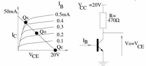
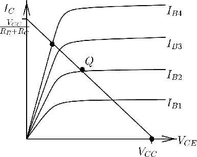
The load line represents the bias conditions in which the dependence is linear;(i.e.: a constance Resistance). Setting up a circuit which changes the transistor bias along the load line means that the transistor is behaving like a resistor.
Consider the collector-Emitter side of the transistor below.
Kirchoff's loops theorem is
A graph of is a line with a slope of and a y-intercept of .
If then .
The point Q_0 in the above curve represents a "Quiescent" (quiet) point where the best amplification occurs because it is in the middle of the operating point. If you are designing an AC amplifier you will want to be at this point to have a wide amplifier range.
If you want to use the transistor for an analog signal (microphone-speaker) then you will want to operate the circuit near Q_0 and have a shallow load line.
Q_0 is the cutoff point where there is no output:ie; the base current is zero; the transistor has infinite resistance
Q_S is the point where the amplifier is saturating. The transistor is supplying its max current a signal going beyond will essentially be clipped. The transistor has an effective resistance of zero at this point.
If you want to make a digital switch then you want the load line as steep as possible so the circuit changes from Q_0 (off) to Q_S(on) as fast as possible.
Temperature Dependence
The voltage drop is a reverse voltage drop for the majority charge carriers BUT a forward voltage for the minority carriers.
As the temperature increases the impurity atoms tend to diffuse through the semiconductor from high concentration regions to low concentration regions.
This means that for a pnp transistor, the thermally created electrons in the n-type base semiconductor will move towards the p-type emitter by crossing the base-emitter junction due to the forward voltage.
Similarly thermally excited holes in the p-type collector will flow to the p-type emitter due to the reverse voltage drop.
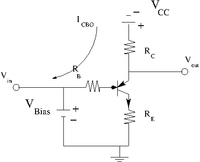
- The reverse current from the Collector to the Base with the emitter Open
The total current becomes
The collector current increases and as a result the transistor temperature increases
The base current becomes
So the base current becomes less but it is usually kept constant by the power source.
You have "thermal runaway" and the transistor may burn out.
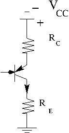
To compensate for this increase you add a resistor to the emitter which hold constant.
As increases with temperature, the base voltage becomes more positive (the increase increases and thus you need less to overcome the the base-emitter junction).
As goes more positive, and increase. But since , will increase.
Bipolar Transistor Amplifier
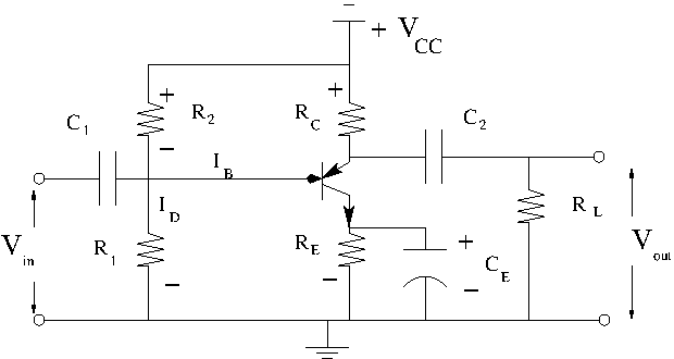
A npn bipolar transistor amplifier configured with a common emitter is shown below.
Let's build this circuit starting with the above load line circuit that has been stabilized for temperature.
Let's add an input current for the base.
Setting I_B
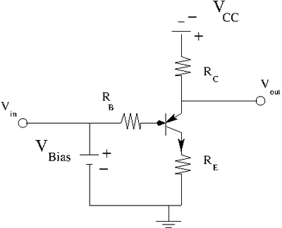
In the above circuit there is a DC bias voltage and an AC input. (The pulse generator in your lab has a DC offset you can use with the AC output sine wave).
In you lab you will want to set an using the DC bias and a in order to put you in the middle of a load line. The AC input will move along that load line.
Applying Kirchoff's loop theorem on the left loop I would have
I have combined the DC bias and the AC input to a total input voltage V_{in}
Since
If you know
and
Then you can set using for a given range of
If you re-derive the load line equation considering the additional resistor R_E then
Kirchoff's law
assume
- Note
In the actual circuit is replaced by 2 resistors ( and ) that provide the input bias voltage by forming a voltage divider using .
In other words
Determining R_E
Using Kirchoff's loop theorem again
General Observations
1.) Notice the input goes through a high pass filter with a break point of.
2.) The output also goes through a high pass filter with a break point of.
3.) Kirchoff voltage rule
4.) Kirchoff law
5.) INput resistance
6.)
