Difference between revisions of "TF EIM Chapt6"
(Replaced content with ' Forest_Electronic_Instrumentation_and_Measurement') |
|||
| Line 1: | Line 1: | ||
| + | ==Load Line== | ||
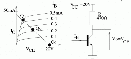
| + | The load line represents the bias conditions in which the <math>I_C -vs V_{CE}</math> dependence is linear;(i.e.: a constance Resistance). Setting up a circuit which changes the transistor bias along the load line means that the transistor is behaving like a resistor. | ||
| + | |||
| + | |||
| + | Consider the collector-Emitter side of the transistor below. | ||
| + | |||
| + | [[File:TF_EIM_LoadLineCircuit1.gif | 500 px]] | ||
| + | |||
| + | |||
| + | Kirchoff's loops theorem is | ||
| + | |||
| + | <math>V_{CC} - I_CR_C -V{CE} = 0</math> | ||
| + | |||
| + | <math>\Rightarrow</math> | ||
| + | |||
| + | <math>I_C = \frac{V_{CC}}{R_C} - \frac{1}{R_C} V_{CE}</math> | ||
| + | |||
| + | A graph of <math>I_C -vs- V_{CE}</math> is a line with a slope of<math> - \frac{1}{R_C}</math> and a y-intercept of <math>\frac{V_{CC}}{R_C}</math>. | ||
| + | |||
| + | If <math>I_C=0</math> then <math>V_{CE} = V_{CC}</math>. | ||
| + | |||
| + | ==Temperature Dependence== | ||
| + | |||
| + | |||
| + | As the temperature increases the impurity atoms tend to diffuse through the semiconductor fro high concentration regions to low concentration regions. | ||
| + | |||
| + | This diffusion changes the<math> I_C -vs- V_{CE}</math> curve near the saturation region because the diode biasing voltages change. | ||
| + | |||
| + | |||
| + | |||
| + | You don't want the temperature change of the transistor to change the bias conditions of the transistor. | ||
| + | |||
| + | =Bipolar Transistor Amplifier= | ||
| + | |||
| + | |||
| + | [[File:TF_EIM_Lab14a.png]] | ||
| + | |||
| + | |||
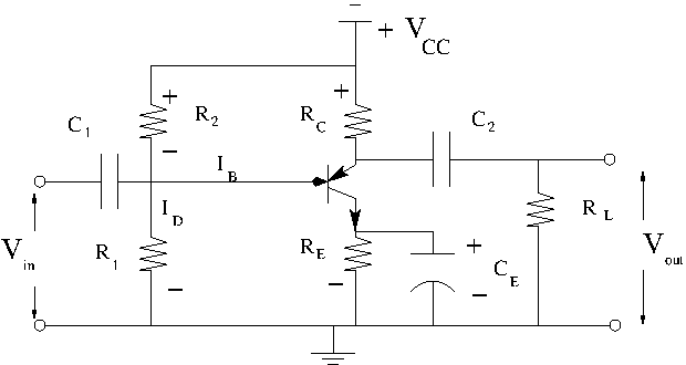
| + | Consider the above circuit. | ||
| + | |||
| + | Observations | ||
| + | |||
| + | 1.) Notice the input goes through a high pass filter with a break point of<math> \frac{1}{R_1 C_1}</math>. | ||
| + | |||
| + | 2.) The output also goes through a high pass filter with a break point of<math> \frac{1}{R_l C_2}</math>. | ||
| + | |||
| + | 3.) Kirchoff voltage rule | ||
| + | |||
| + | :<math>V_{CC} -I_C R_C - V_{CE} - I_E R_E = 0</math> | ||
| + | :<math>V_{CC} - V_{CE} -I_C (R_C + R_E) = 0</math> <math>I_C \approx I_E</math> | ||
| + | |||
| + | :<math>\Rightarrow I_C =\frac{ V_{CC} - V_{CE}}{R_C + R_E }</math> | ||
| + | |||
| + | 4.) Kirchoff law | ||
| + | |||
| + | :<math>V_{CC} -(I_B + I_D) R_2 - V_{EB} - I_E R_E = 0</math> | ||
| + | |||
| + | 5.) INput resistance | ||
| + | |||
| + | <math>\frac{1}{R_{in}} = \frac{1}{X_B} + \frac{1}{R_1} + \frac{1}{R_2}</math> | ||
| + | |||
| + | 6.) | ||
| + | |||
| + | :<math>V_B = \frac{R_1}{R_1+R_2} V_{CC}</math> | ||
[[Forest_Electronic_Instrumentation_and_Measurement]] | [[Forest_Electronic_Instrumentation_and_Measurement]] | ||
Revision as of 01:34, 16 March 2011
Load Line
The load line represents the bias conditions in which the dependence is linear;(i.e.: a constance Resistance). Setting up a circuit which changes the transistor bias along the load line means that the transistor is behaving like a resistor.
Consider the collector-Emitter side of the transistor below.
Kirchoff's loops theorem is
A graph of is a line with a slope of and a y-intercept of .
If then .
Temperature Dependence
As the temperature increases the impurity atoms tend to diffuse through the semiconductor fro high concentration regions to low concentration regions.
This diffusion changes the curve near the saturation region because the diode biasing voltages change.
You don't want the temperature change of the transistor to change the bias conditions of the transistor.
Bipolar Transistor Amplifier
Consider the above circuit.
Observations
1.) Notice the input goes through a high pass filter with a break point of.
2.) The output also goes through a high pass filter with a break point of.
3.) Kirchoff voltage rule
4.) Kirchoff law
5.) INput resistance
6.)

