Difference between revisions of "Warren Parsons MS Thesis"
| Line 18: | Line 18: | ||
|} | |} | ||
| + | |||
| + | = Complete Thesis = | ||
| + | |||
| + | [[Media:MastersThesis.pdf]] | ||
= Required thesis changes= | = Required thesis changes= | ||
Revision as of 06:05, 14 June 2010
| Date | Task |
| 9/16/09 | Finalize Committee |
| 2/25/10 | Stuff V4 Breakout Box |
| 3/23/10 | Working Breakout Box |
| 5/20/2010 | S- curve automation |
| 4/13/09 | Complete Draft of entire Thesis |
| 4/23/10 | Make changes,Schedule Defense, and send copies to committee members (2 weeks to finish paperwork after defense) |
Complete Thesis
Required thesis changes
1.) Add a conclusion
2.) work on description in pg 42
2.) Need S_curves and performance measurements.
Thesis Chapters
Abstract
Chapter 1 Introduction
Chapter 2 V1495 Module by CAEN
Chapter 3 Readout Controller Library
File:Readout Controller Library.pdf
Chapter 4 VFAT Breakout Board
Chapter 5 Conclusion
Bibliography
Appendix
Do we want to include all of the source code and other various items in an appendix or do we want to simply include them in a CD along with the thesis?
Detector description
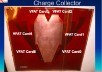
Charge collector
Output connector
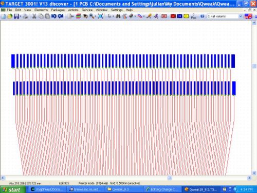
Strips - Output connector roadmap
A close up view of the 130 pin pads which will be used to mount connectors for the VFAT_readout_electronics.
P5KS 130 pin 6.5 mm Panasonic connectors
We need to have plated holes which allow the copper lines to pass through to the very last layer where the copper pads for the 130 pin connector are.
Chapt V1495
v1495usr.vhd
- GEMReadout.vhd
The following is the UML for the GEMReadout module:
- GEMReadout_tb.vhd
- GEMRxChannel.vhd
The following is the UML for the GEMRxChannel module:
- GEMRxEventDataFIFO.vhd
- a routine controlling the FIFO
- GEMRxEventSizeFIFO.vhd
- Defines the Event size and structure
- GEMTxChannel.vhd
The following is the UML for the GEMTxChannel module:
- PLLVBlock.vhd
- spare_if_rtl.vhd
- tristate_if_trl.vhd
- v1495usr.vhd
- v1495usr_pkg.vhd
- GEMTrigger.vhd
The following is the UML diagram for the GEMTrigger module:
- v1495usr_hal.vqm
- From the v1495 manual this is the v1495 Hardware Abstraction Layer. It is an HDL module provided in Verilog format at the netlist level in order to help interface the hardware.
- Reading through this file makes it clear that we are using the Cyclone chip family. I can't find where the "cyclone_lcell" module is defined. I am wondering if it is defined inside of the Quartus II program in a library somewhere. Figuring this out would probably help unravel how our HDL code is actually instantiated in hardware.
General introduction to the readout scheme
Readout Blockdiagram
Changing MCLK frequency
Output MCLK and Level 1 Trigger
VFAT input port
V1495 Data format
CODA Readout
The V1495 module transfers data 16 bits at a time to the ROC. An array within the ROC memory will be filled with the V1495 data stream 16 bits at a time to optimize data throughout. The array within the ROC memory will then be transferred to the host computer and stored.
Move the source code to an appendix
Readout list
CODA Data Format
QwAnalaysis
Calibration Pulse Experiment and Results
The following are the parameters that were used for the Calibration Pulse experiment.
MCLK = 40Mhz IPreampIn 0xa8 IPreampFeed 0x50 IPreampOut 0x96 IShaper 0x96 IShaperFeed 0x64 IComp 0x78
MSPulseLength<2:0> = 0x0 // MonoStable pulse length of 1 clock period
HitCountSel<3:0> = 0x0 // Fast-OR of all 128 channels
The MCLK frequency was chosen because it is at which the original Calibration pulse experiments were run. Also, in the experiment the CalPulse signal supposedly has a peaking time of 22ns. Thus, if we want to have any hope of catching the calibration pulse, we will most likely need to run at at least 40 Mhz. This, of course, also depends on the peak amplitude of the pulse as well as how long its tail is.
The v1495 firmware performs a straight pass-through of the trigger signal from the pattern generator. Care has been taken to make sure that the signals are passed along while they are stable rather than at a transition. Also, it is known that the MCLK shown in Figure 10 of the VFAT manual is out of phase by 180o, thus care has also been taken to make sure that the T1 signal has the proper phase with respect to MCLK. This whole process causes the signal being output to be one clock cycle behind the signal being injected; this shouldn't be a problem.
The "TRIGGER OUT" signal is used as the MCLK for the VFATs and "OUTPUT1" as the T1 signal for the VFAT. OUTPUT1 is set such that it will output the Calpulse signal followed by a single break pulse and then followed by the LV1A signal. The pattern is long enough that we should be able to see whether we received any hits on the lines that we have CalChan turned on in the respective ChanReg. Right now the experiment is running too quickly and does not have the proper setup to see whether the HitCount registers are working properly with the calibration pulses being sent.

