Difference between revisions of "TF EIM Chapt9"
| (60 intermediate revisions by 2 users not shown) | |||
| Line 41: | Line 41: | ||
[[File:TF_EIM_BiPolarOpAmp.png]] | [[File:TF_EIM_BiPolarOpAmp.png]] | ||
| + | |||
| + | ==Op Amp current and voltage rules== | ||
| + | |||
| + | The simple rules used when analzing Op Amp circuits are | ||
| + | |||
| + | 1.) The current into each input Op Amp terminals is Zero | ||
| + | |||
| + | 2.) The voltage difference between the two input terminal is Zero. <math>V_1 = V_2</math> | ||
| + | |||
| + | : Note the impact of Rule 2 is that the open loop gain <math>A_0 = \frac{V_{out}}{V_2-V_1} = \infty</math> | ||
=Inverting Amplifier= | =Inverting Amplifier= | ||
| Line 52: | Line 62: | ||
Applying the current junction rule at the inverting terminal one would have. | Applying the current junction rule at the inverting terminal one would have. | ||
| − | :<math>I_1</math>= current through resistor <math>R_1</math> = \frac{ V_1-V_{in}}{R_1} | + | :<math>I_1</math>= current through resistor <math>R_1</math> =<math> \frac{ V_1-V_{in}}{R_1}</math> |
:<math>I_2</math> = current through <math>R_2</math> = <math>\frac{V_{out}-V_1}{R_2}</math> | :<math>I_2</math> = current through <math>R_2</math> = <math>\frac{V_{out}-V_1}{R_2}</math> | ||
:<math>I_{B1}</math> = current entering the inverting terminal <math>V_1</math> (the base of the bipolar transistor) | :<math>I_{B1}</math> = current entering the inverting terminal <math>V_1</math> (the base of the bipolar transistor) | ||
| − | Current conservation \Rightarrow | + | Current conservation<math> \Rightarrow</math> |
| − | :<math>I_1 | + | :<math>I_2 = I_1 + I_{B1}</math> |
or | or | ||
| − | :<math>\frac{ | + | :<math>\frac{V_{out}-V_1}{R_2} = \frac{ V_1-V_{in}}{R_1} +I_{B1}</math> |
| − | A "perfect" Op Amp has I_{B1} = 0 | + | A "perfect" Op Amp has <math>I_{B1} = 0</math> |
| − | :<math>\frac{ | + | :<math>\frac{V_{out}-V_1}{R_2} = \frac{ V_1-V_{in}}{R_1}</math> |
Using the equivalent circuit from above | Using the equivalent circuit from above | ||
| − | <math>V_{out} = | + | <math>V_{out} = A_0(V_2 - V_1)</math> |
| + | |||
| + | Since <math>V_2 = 0</math> for the inverting amplifier circuit above | ||
| + | |||
| + | :<math>\frac{V_{out}+\frac{V_{out}}{A_0}}{R_2}=\frac{ -\frac{V_{out}}{A_0}-V_{in}}{R_1} </math> | ||
| + | |||
| + | :<math>\Rightarrow \frac{1+\frac{1}{A_0}}{R_2} = \frac{ -\frac{1}{A_0}-\frac{V_{in}}{V_{out}}}{R_1} </math> | ||
| + | |||
| + | |||
| + | <math>\frac{V_{in}}{V_{out}} =-\frac{1}{A_0}-R_1 \frac{1+\frac{1}{A_0}}{R_2}</math> | ||
| + | :<math>= -\frac{R_2}{A_0R_2}-R_1 \frac{A_0+1}{A_0R_2}</math> | ||
| + | :<math>= -\frac{R_2 + R_1 (A_0+1)}{A_0R_2}</math> | ||
| + | |||
| + | : Gain<math>\equiv \frac{V_{out}}{V_{in}} = - \frac{A_0 R_2}{R_1(A_0+1) + R_2} \approx - \frac{R_2}{R_1}</math> : if<math> R_1 \ll R_2</math> and <math>A_0 >> 1</math> | ||
| + | |||
| + | ;The "-" sign means that the output is 180 degrees out of phase with the input. | ||
| + | |||
| + | This inverting amplifier has a gain which depends only on the ratio of resistors as long as the open-loop gain <math>A_0</math> is a lot larger then unity and<math> R_2</math> is a lot larger than <math>R_1</math> (negative feedback). | ||
| + | |||
| + | ==NonZero input bias current I_B== | ||
| + | |||
| + | Consider what happens if the terminal current is not zero (ie the Op Amp isn't perfect) | ||
| + | |||
| + | Returning back the the junction rule | ||
| + | |||
| + | |||
| + | :<math>I_2 = I_1 + I_{B1}</math> | ||
| + | |||
| + | :<math> \frac{V_{out}-V_1}{R_2} =\frac{ V_1-V_{in}}{R_1}+I_{B1}</math> | ||
| + | |||
| + | assuming for a minute that V_1=V_2 = 0 (first Op AMp rule is broken but second rule holds) | ||
| + | |||
| + | then | ||
| + | |||
| + | :<math>V_{out}=-\frac{R_2}{R_1} V_{in} + I_{B1}R_2</math> | ||
| + | |||
| + | |||
| + | If <math>V_{in} >> I_{B1}R_2</math> then your Op Amp will operate close to a perfect one. | ||
| + | |||
| + | ===input bias offset current=== | ||
| + | |||
| + | The bias current <math>I_{B1}</math> offsets the output voltage <math>V_{out}.</math> | ||
| + | |||
| + | If we can find a way to cancel out this offset then we will be essentially "nulling" the bias current <math>I_{B1}</math> so the Op Amp is more "perfect". | ||
| + | |||
| + | |||
| + | You can do this by using the other half of the amplifier, the non-inverting input current <math>I_{B2}</math>. | ||
| + | |||
| + | If you use a pull up resister (<math>R_3)</math> to raise the non-inverting input from ground then there will be a potential difference created from the current <math>I_{B2}</math> | ||
| + | |||
| + | |||
| + | If <math>V_{in} = 0</math> then | ||
| + | |||
| + | <math>V_{out} = I_{B1}R_2</math> | ||
| + | |||
| + | using the equivalent circuit description | ||
| + | |||
| + | <math>Gain = \frac{V_{out}}{V_2-V_1} \Rightarrow V_2 Gain = V_{out}</math> | ||
| + | |||
| + | So to cancel the I<math>_{B1}R_2</math> offset in<math> V_{out}</math> you supply the opposite current with a voltage offset. | ||
| + | |||
| + | :<math>Gain V_2 = - I_{B1}R_2</math> | ||
| + | |||
| + | <math>V_2 = -I_{B2}R_3</math> | ||
| + | |||
| + | Gain =<math> \left ( 1 + \frac{R_2}{R_1} \right)</math> = gain for the non-inverting input (V_2) | ||
| + | |||
| + | \Rightarrow | ||
| + | |||
| + | <math>-I_{B2}R_3 \left ( 1 + \frac{R_2}{R_1} \right) = - I_{B1}R_2</math> | ||
| + | |||
| + | or if <math>I_{B2} = I_{B1}</math> | ||
| + | |||
| + | <math>R_3 = \frac{R_1 R_2}{R_1+R_2}</math> | ||
| + | |||
| + | |||
| + | <math>I_{io} \equiv I_{B2} - I_{B1} \approx 0 </math> = input bias offset current. | ||
| + | |||
| + | ===Input Offset Voltage=== | ||
| + | |||
| + | |||
| + | The second rule of the perfect Op Amp is that the voltage difference between the input terminals is zero (the Op Amp voltage rule). | ||
| + | |||
| + | For the typical inverting Op Amp you can imagine that a voltage difference exists at terminal <math>V_1</math>. | ||
| + | |||
| + | Let | ||
| + | |||
| + | <math>V_{io}</math> = input offset voltage source on terminal<math> V_1</math>. | ||
| + | |||
| + | |||
| + | If <math> V_{in} =0</math> | ||
| + | |||
| + | Then the inverting amplifier looks like a voltage divider with<math> V_{out}</math> being stepped down to <math>V_{io}</math> through the resistor <math>R_2</math>. | ||
| + | |||
| + | <math>V_{out} -I_(R_1+R_2) =0 \Rightarrow I = \frac{V_{out}}{R_1 + R_2}</math> | ||
| + | |||
| + | <math>V_{io} - I R_1= 0 \Rightarrow V_{io} = I R_1 = \frac{V_{out}}{R_1 + R_2} R_1</math> | ||
| + | |||
| + | : <math>V_{out} = \frac{R_2}{R_1+R_2} V_{io} = \left ( 1 + \frac{R_2}{R_1} \right ) V_{io}</math> | ||
| + | |||
| + | : A direct measurement of <math>V_{io}</math> can be made if you set <math>R_2</math> to give you a large gain and have <math>V_{in}</math> = 0 (no input). What you measure at <math>V_{out}</math> will be <math>V_{io}</math>. | ||
| + | |||
| + | ===Vout=== | ||
| + | |||
| + | For a non-perfect Op Amp | ||
| + | |||
| + | :<math>V_{out} = - \frac{A_0 R_2}{R_1(A_0+1) + R_2} V_{in} + I_{B1}R_2 + \left ( 1 + \frac{R_2}{R_1} \right ) V_{io}</math> | ||
| + | ::<math>\approx - \left( \frac{R_2}{R_1} \right)V_{in} + I_{B1}R_2 + \left ( 1 + \frac{R_2}{R_1} \right ) V_{io}</math> | ||
| + | |||
| + | ; V_{io} can be either > 0 or < 0. | ||
| + | |||
| + | ==Slew Rates== | ||
| + | |||
| + | The Slew Rate is defined as the maximum rate at which the Op AMp voltage can change. | ||
| + | |||
| + | This can be observed as an increase in the rise time of an input pulse (a Capacitive effect). | ||
| + | |||
| + | If the AC input to an Op Amp is a square wave then as the frequency increases you will start to see the square wave input become rounded. | ||
| + | |||
| + | The Slew rate is the voltage swing divided by the amount of time needed to make that swing (ie the slope of the Voltage -vs- time plot). | ||
| + | |||
| + | |||
| + | You can then calculate the mximum input frequency which will be free of distortion using this Slew Rate | ||
| + | |||
| + | : <math>\nu = \frac{Slew Rate}{2 \pi \Delta V}</math> | ||
| + | |||
| + | Where <math>\Delta V</math> = peak -to - peak voltage swing of your input signal. | ||
| + | |||
| + | |||
| + | How do you get the above? | ||
| + | |||
| + | Assum your input signal is a cosine wave and take the derivative to get the slew rate | ||
| + | |||
| + | Slew Rate <math>\equiv \left ( \frac{V}{t} \right )_{max} = \left . \omega V_0 \cos (\omega t) \right |_{max} = 2 \pi \nu V_0</math> | ||
| + | |||
| + | ==PSRR (Power Supply Rejection Ratio== | ||
| + | |||
| + | |||
| + | The ripple of a DC power supply to an Op Amp can produce a ripple on the Op Amp output. | ||
| + | |||
| + | This is because changes in the power supply voltage result in changes in the input offset voltage (V_{io}) | ||
| + | |||
| + | |||
| + | The output voltage from the inverting and non-inverting Op AMp is given by | ||
| + | |||
| + | :<math>V_{out} = \left ( 1 + \frac{R_2}{R_1}\right ) V_{io}</math> | ||
| + | |||
| + | :<math>\Rightarrow \Delta V_{out} = \left ( 1 + \frac{R_2}{R_1}\right ) \Delta V_{io}</math> | ||
| + | :: <math>= \left ( 1 + \frac{R_2}{R_1}\right ) \left ( PSRR \Delta V_{cc} \right )</math> | ||
| + | |||
| + | where | ||
| + | |||
| + | :<math>PSSR \equiv \frac{\Delta V_{io}}{\Delta V_{cc}}</math> | ||
| + | |||
| + | |||
| + | To measure PSRR you set<math> V_{in}</math> to zero (no input) then measure <math>V_{out}</math> for several <math>V_{cc}</math>. | ||
| + | |||
| + | A plot of <math>\Delta V_{out} -vs \Delta V_{cc}</math> will have a slope that relates to PSSR. | ||
| + | |||
| + | ==Op Amp Noise== | ||
| + | |||
| + | |||
| + | The noise that an Op Amp produces at its output is dependent on the noise that is injected by its input and the Gain of the Op Amp. | ||
| + | |||
| + | In the inverting Op Amp circuit you have 2 resistors which determine the Gain. Resistors have an intrinsic noise, called Johnson noise, which is due to their temperature. Electrons traversing the resistor, although they are being directed by an electric field, will have thermal energy that results in a fluctuation in the voltage difference across the ends of the resistor. | ||
| + | |||
| + | J.B. Johnson found that the square of the noise voltage varies linearly with the resistance. He also showed that the power associated with the fluctuations varied linearly with the bandwidth of the measuring instrument. Or in General | ||
| + | |||
| + | :<math>\bar{V_n^2} = 4kTRB_w</math> | ||
| + | |||
| + | where | ||
| + | |||
| + | <math>V_n</math> = the noise voltage | ||
| + | |||
| + | <math>B_W</math> = bandwidth of measuring insturment | ||
| + | |||
| + | k = Boltzman's contant | ||
| + | |||
| + | T=Temperature | ||
| + | |||
| + | So the RMS noise is given as | ||
| + | |||
| + | :<math>V_{ns} \equiv \sqrt{\bar{V_n^2}} = \sqrt{4kTRB_w}</math>= noise voltage | ||
| + | |||
| + | <math>\Rightarrow</math> Resistor Noise = <math>\sqrt{4kTR} = \frac{V_{ns}}{\sqrt{B_W}} = Volts / sqrt{Hz}</math> | ||
| + | |||
| + | |||
| + | Another source of Noise is the noise from the source driving the Op Amp | ||
| + | :<math>V_{ns} \equiv</math> noise instrinsic to the source driving the Op Amp | ||
| + | |||
| + | The third source of noise is the current which traverses the two Op Amp inputs through the internal resistance of the Op Amp (R_{in}). | ||
| + | |||
| + | :V_{ni} = i_n R_{in} = internal noise of the amplifier | ||
| + | |||
| + | So the total noise of the amplifier is given as | ||
| + | |||
| + | :<math>V_{ntot} = \sqrt{V_n^2 + V_{ni}^2 + V_{ns}^2}</math> | ||
| + | |||
| + | This noise gets amplified by the Op Amp and modulated by the Band width such that | ||
| + | |||
| + | <math>V_{no} = V_{ntot} Gain \sqrt{B_W} = \sqrt{V_n^2 + V_{ni}^2 + V_{ns}^2} Gain \sqrt{B_W}</math> | ||
| − | |||
| − | + | [[Forest_Electronic_Instrumentation_and_Measurement]] | |
Latest revision as of 16:45, 20 April 2011
Operational Amplifiers (Op Amps)
The operational amplifier is monolithic (single chip) integrated circuit composed of transistors, resistors, diodes, and other components.
The small package produces a device with small capacitance and inductance which is superior to assembling the equivalent circuit with individual components.
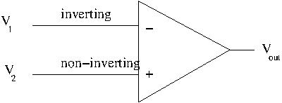
Op-Amp
the "-" sign indicates the inverting input terminal and the "+" indicates the non-inverting input.
A positive going input voltage at the non-inverting ("+") input produces a positive going output.
A positive going input voltage at the inverting ("+") input produces a negative going output.
In other words the output is in phase when the input is non-inverting and 180 degrees out of phase when the input is inverting.
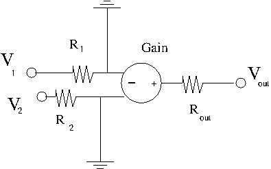
Equivalent circuit
Gain = Open loop gain = gain when there isn't anything hooked up to the op amp to draw current from it.
Common Mode
Common mode input is defined as the situation where the two inputs are equal (. In this case is inverted and will cancel the input so the output becomes Zero in the ideal Op Amp.
Op Amps usually has two bias supplies in order to produce a high gain as determined by the difference in the input voltages. The output can't be larger than the supply bias.
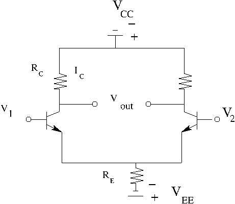
Differential Op Amp
A single stage differential op Amp can be described as being composed of two bipolar transistors in a common emitter configuration as shown below.
Op Amp current and voltage rules
The simple rules used when analzing Op Amp circuits are
1.) The current into each input Op Amp terminals is Zero
2.) The voltage difference between the two input terminal is Zero.
- Note the impact of Rule 2 is that the open loop gain
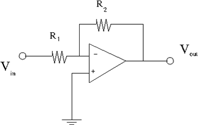
Inverting Amplifier
The above circuit is called an inverting amplifier. The input signal is applied to the inverting terminal ("-", , or) of the Op Amp through a resister R_1. The non-inverting terminal ("+",, or ) is grounded.
Applying the current junction rule at the inverting terminal one would have.
- = current through resistor =
- = current through =
- = current entering the inverting terminal (the base of the bipolar transistor)
Current conservation
or
A "perfect" Op Amp has
Using the equivalent circuit from above
Since for the inverting amplifier circuit above
- Gain : if and
- The "-" sign means that the output is 180 degrees out of phase with the input.
This inverting amplifier has a gain which depends only on the ratio of resistors as long as the open-loop gain is a lot larger then unity and is a lot larger than (negative feedback).
NonZero input bias current I_B
Consider what happens if the terminal current is not zero (ie the Op Amp isn't perfect)
Returning back the the junction rule
assuming for a minute that V_1=V_2 = 0 (first Op AMp rule is broken but second rule holds)
then
If then your Op Amp will operate close to a perfect one.
input bias offset current
The bias current offsets the output voltage
If we can find a way to cancel out this offset then we will be essentially "nulling" the bias current so the Op Amp is more "perfect".
You can do this by using the other half of the amplifier, the non-inverting input current .
If you use a pull up resister ( to raise the non-inverting input from ground then there will be a potential difference created from the current
If then
using the equivalent circuit description
So to cancel the I offset in you supply the opposite current with a voltage offset.
Gain = = gain for the non-inverting input (V_2)
\Rightarrow
or if
= input bias offset current.
Input Offset Voltage
The second rule of the perfect Op Amp is that the voltage difference between the input terminals is zero (the Op Amp voltage rule).
For the typical inverting Op Amp you can imagine that a voltage difference exists at terminal .
Let
= input offset voltage source on terminal.
If
Then the inverting amplifier looks like a voltage divider with being stepped down to through the resistor .
- A direct measurement of can be made if you set to give you a large gain and have = 0 (no input). What you measure at will be .
Vout
For a non-perfect Op Amp
- V_{io} can be either > 0 or < 0.
Slew Rates
The Slew Rate is defined as the maximum rate at which the Op AMp voltage can change.
This can be observed as an increase in the rise time of an input pulse (a Capacitive effect).
If the AC input to an Op Amp is a square wave then as the frequency increases you will start to see the square wave input become rounded.
The Slew rate is the voltage swing divided by the amount of time needed to make that swing (ie the slope of the Voltage -vs- time plot).
You can then calculate the mximum input frequency which will be free of distortion using this Slew Rate
Where = peak -to - peak voltage swing of your input signal.
How do you get the above?
Assum your input signal is a cosine wave and take the derivative to get the slew rate
Slew Rate
PSRR (Power Supply Rejection Ratio
The ripple of a DC power supply to an Op Amp can produce a ripple on the Op Amp output.
This is because changes in the power supply voltage result in changes in the input offset voltage (V_{io})
The output voltage from the inverting and non-inverting Op AMp is given by
where
To measure PSRR you set to zero (no input) then measure for several .
A plot of will have a slope that relates to PSSR.
Op Amp Noise
The noise that an Op Amp produces at its output is dependent on the noise that is injected by its input and the Gain of the Op Amp.
In the inverting Op Amp circuit you have 2 resistors which determine the Gain. Resistors have an intrinsic noise, called Johnson noise, which is due to their temperature. Electrons traversing the resistor, although they are being directed by an electric field, will have thermal energy that results in a fluctuation in the voltage difference across the ends of the resistor.
J.B. Johnson found that the square of the noise voltage varies linearly with the resistance. He also showed that the power associated with the fluctuations varied linearly with the bandwidth of the measuring instrument. Or in General
where
= the noise voltage
= bandwidth of measuring insturment
k = Boltzman's contant
T=Temperature
So the RMS noise is given as
- = noise voltage
Resistor Noise =
Another source of Noise is the noise from the source driving the Op Amp
- noise instrinsic to the source driving the Op Amp
The third source of noise is the current which traverses the two Op Amp inputs through the internal resistance of the Op Amp (R_{in}).
- V_{ni} = i_n R_{in} = internal noise of the amplifier
So the total noise of the amplifier is given as
This noise gets amplified by the Op Amp and modulated by the Band width such that


