Difference between revisions of "VFAT readout electronics"
| (132 intermediate revisions by 2 users not shown) | |||
| Line 1: | Line 1: | ||
| − | This page describes the GEM detector readout system | + | =Description= |
| + | This page describes the GEM detector readout system. The system has four components, the VFAT readout card from CERN, a signal breakout box, a Gumstick I2C control computer, and an I/O VME module to record the LVDS output from the VFAT card. | ||
| + | |||
| + | ==Readout Scheme overview== | ||
| + | |||
| + | [[File:VFATReadoutOverview_082211.png| 400 px]] | ||
| + | |||
| + | |||
| + | {| border="1" cellpadding="4" | ||
| + | |- | ||
| + | | Module||Desc | ||
| + | |- | ||
| + | | [[https://wiki.iac.isu.edu/index.php/CAEN_V1495_IO V1495]]|| An FPGA to source the MCLK and Trig signals as well as record the VFAT LVDS output. An external clock is used to drive the MCLCK pulse. | ||
| + | |- | ||
| + | | Power and I2C || A custom NIM module which houses a [[VFAT_readout_electronics#Power_supply]] and a [[VFAT_readout_electronics#Gumstick_I2C_controller]] used for I2C controls | ||
| + | |- | ||
| + | | Breakout board|| A custom board used as a branch highway for both the LVDS and I2C signals to and from up to 6 VFAT cards. [https://wiki.iac.isu.edu/images/7/7e/MastersThesis.pdf Warren Parson Thesis] describing most of the system. | ||
| + | |- | ||
| + | | VFAT ||[https://wiki.iac.isu.edu/index.php/VFAT_readout_electronics#VFAT_Board_specifications VFAT readout Card] | ||
| + | |} | ||
| + | |||
| + | =New Parts Order List for Rev 4= | ||
| + | |||
| + | 20 1uF 805 Capacitors | ||
| + | http://search.digikey.com/scripts/DkSearch/dksus.dll?Detail&name=490-1695-1-ND | ||
| + | |||
| + | 20 80Ohm Common-mode filters | ||
| + | http://search.digikey.com/scripts/DkSearch/dksus.dll?Detail&name=240-2475-1-ND | ||
| + | |||
| + | 20 150Ohm Common-mode filters | ||
| + | http://search.digikey.com/scripts/DkSearch/dksus.dll?Detail&name=240-2473-1-ND | ||
| + | |||
| + | (I'm not sure which of these will work best yet.) | ||
| + | |||
| + | 5(ish) BNC Female Sockets | ||
| + | http://search.digikey.com/scripts/DkSearch/dksus.dll?Detail&name=A32260-ND | ||
| + | |||
| + | 10(ish) BNC Male Connectors | ||
| + | http://search.digikey.com/scripts/DkSearch/dksus.dll?Detail&name=A24483-ND | ||
| + | |||
| + | (You might have a better idea for the BNC items, however.) | ||
| + | |||
| + | We also need larger-valued resistors for the LEDs on the board, but I'd have to look at the new circuit board again to get these values. I get this first thing tomorrow morning. (Unless Brian beats me to it.) | ||
| + | |||
| + | 2 PES51 Soldiering Iron Tips... | ||
| + | |||
| + | 1 of these | ||
| + | http://search.digikey.com/scripts/DkSearch/dksus.dll?Detail&name=ETA-ND | ||
| + | |||
| + | And 1 of the slightly smaller version | ||
| + | http://search.digikey.com/scripts/DkSearch/dksus.dll?Detail&name=ETH-ND | ||
| + | |||
| + | 50 Jumpers: | ||
| + | http://search.digikey.com/scripts/DkSearch/dksus.dll?Detail&name=3M9580-ND | ||
=VFAT readout Block Diagram= | =VFAT readout Block Diagram= | ||
| Line 6: | Line 59: | ||
A VFAT board from CERN is evaluated for use as a readout board to convert the GEM output analog signal to a digital signal. | A VFAT board from CERN is evaluated for use as a readout board to convert the GEM output analog signal to a digital signal. | ||
| − | + | :::[[Image:BreakOutBox.jpg | 500 px]] | |
| − | + | ||
| − | + | :::[[Image:VFAT_Breakout_REV3.png | 700 px]] | |
| − | + | ||
| − | + | :::[[Image:VFAT_Breakout_REV3_Design_Schematic.png | 700 px]] | |
| − | + | ||
| − | + | <br>[[Media:BreakOutBox.text]] | |
| − | + | ||
| − | + | [[Breakout Board Design]] | |
| − | + | ||
| + | |||
| + | === RJ45 I2C + Power connector === | ||
| + | |||
| + | {| border="1" cellpadding="4" | ||
| + | |- | ||
| + | | Pin || RJ45 Color Code|| |VFAT color Code/ Pin Number ||Desc | ||
| + | |- | ||
| + | | 1 ||white with orange spots || B25 || Analog Ground | ||
| + | |- | ||
| + | | 2 ||solid orange|| A25 || Analog Vcc | ||
| + | |- | ||
| + | | 3 || white with green|| A7 || Hard Reset goes to +Vcc | ||
| + | |- | ||
| + | | 4 ||solid blue || A2 || SCL | ||
| + | |- | ||
| + | | 5 ||white with blue || B2|| SDA | ||
| + | |- | ||
| + | | 6 || green || not connected | ||
| + | |- | ||
| + | | 7 || white with brown|| B1 ||Digital Ground | ||
| + | |- | ||
| + | | 8 || solid brown || A1 || Digital Vcc | ||
| + | |- | ||
| + | |||
| + | |} | ||
| + | |||
== [http://totem.web.cern.ch/Totem/work_dir/electronics/totelwork_files/PDFgeneral/VFAT2Manual.pdf VFAT Board specifications]== | == [http://totem.web.cern.ch/Totem/work_dir/electronics/totelwork_files/PDFgeneral/VFAT2Manual.pdf VFAT Board specifications]== | ||
| − | Photos of the top and bottom side of the VFAT card are shown below. The top side has a 50 pin connector which goes to the breakout box to separate I2C control signals and LVDS data I/O signals. The bottom side attaches to the GEM detector readout board via a 130 pin | + | Photos of the top and bottom side of the VFAT card are shown below. The top side has a 50 pin connector which goes to the breakout box to separate I2C control signals and LVDS data I/O signals. The bottom side attaches to the GEM detector readout board via a 130 pin [https://panasonic-denko.co.jp/ac/e/control/connector/base-base/specdetail/index.jsp?part_no=AXK5SA3277YG socket connector].<br> |
| − | <center>[[Image:VFATtop.jpg | 200 px]][[Image:VFATbottom.jpg]]</center> | + | <center>[[Image:VFATtop.jpg | 200 px]][[Image:VFATbottom.jpg]][[Image:VFAT_Bottom_HiRes.png|200px]]</center> |
* 40 MHz sampling | * 40 MHz sampling | ||
| Line 48: | Line 127: | ||
===I2C signals=== | ===I2C signals=== | ||
[[I2C]] (Can travel 8 m)<br/> | [[I2C]] (Can travel 8 m)<br/> | ||
| + | |||
| + | |||
| + | Let's try system for 150 ft transmission | ||
| + | |||
| + | ===I2C LED tester=== | ||
| + | |||
| + | The led.arm program turns the led a random color if run with no arguments, or you can specify r, g, b, or a combination of those, in the first argument: | ||
| + | |||
| + | <pre> | ||
| + | |||
| + | ./led.arm #random | ||
| + | ./led.arm r #red | ||
| + | ./led.arm rg #purple | ||
| + | |||
| + | </pre> | ||
| + | |||
| + | Other things that could be tested are looking at the SDA/SCL signal on the vfat cable pulled apart on the breadboard, hooking the led light up to the breakout cable breadboard, or bypassing the breakout board i2c signals to the breadboard. | ||
== Breakout box specs (preliminary) == | == Breakout box specs (preliminary) == | ||
| Line 65: | Line 161: | ||
** ScanIn connector (cascaded) | ** ScanIn connector (cascaded) | ||
** ScanOut connector (cascaded) | ** ScanOut connector (cascaded) | ||
| − | * | + | * RJ45 port to gumstix box containing [[I2C]] and other signals: |
** Power (3.3 or 2.5V) | ** Power (3.3 or 2.5V) | ||
** Ground | ** Ground | ||
| Line 84: | Line 180: | ||
=== Ribbon cable pinouts === | === Ribbon cable pinouts === | ||
| + | |||
| + | The B side of the connector is the same side as the cable polarity notch. | ||
{| border="1" cellpadding="4" | {| border="1" cellpadding="4" | ||
|- | |- | ||
| − | | # || VFAT <br/> pin # || Name || Value || Test rig color <br/> Primary/Second | + | | # || VFAT <br/> pin # || Name || Value || Test rig color <br/> Primary/Second (Bigger color/smaller color) |
|- | |- | ||
| B1 || || DGND || Digital Ground || Black/Grey (shared) | | B1 || || DGND || Digital Ground || Black/Grey (shared) | ||
| Line 101: | Line 199: | ||
| A3 || || DVDD || +2.5V || Red/Grey (shared) | | A3 || || DVDD || +2.5V || Red/Grey (shared) | ||
|- | |- | ||
| − | | B4 || 162 || DACo-V || DAC output Volt | + | | B4 || 162 || DACo-V || DAC output Volt || No Connection |
|- | |- | ||
| − | | A4 || 163 || DACo-I || DAC output Current | + | | A4 || 163 || DACo-I || DAC output Current || No Connection |
|- | |- | ||
| B5 || 164 || I2C ADDR 2 || I2C Address Most || White/Blue | | B5 || 164 || I2C ADDR 2 || I2C Address Most || White/Blue | ||
| Line 113: | Line 211: | ||
| A6 || 169 || REsB || Soft Reset (Program saved) || White/Grey | | A6 || 169 || REsB || Soft Reset (Program saved) || White/Grey | ||
|- | |- | ||
| − | | B7 || 170 || ForceRehOff || ?? bond to grnd | + | | B7 || 170 || ForceRehOff || ?? bond to grnd || No Connection |
|- | |- | ||
| A7 || 171 || REhB || Hard Reset || Grey/White | | A7 || 171 || REhB || Hard Reset || Grey/White | ||
| Line 169: | Line 267: | ||
| A20 || 199 || S1 (+) || || Yellow/Blue | | A20 || 199 || S1 (+) || || Yellow/Blue | ||
|- | |- | ||
| − | | B21 || || DGND || Digital Ground | + | | B21 || || DGND || Digital Ground || No Connection |
|- | |- | ||
| − | | A21 || || DVDD || +2.5V | + | | A21 || || DVDD || +2.5V || No Connection |
|- | |- | ||
| − | | B22 || || DGND || Digital Ground | + | | B22 || || DGND || Digital Ground || No Connection |
|- | |- | ||
| − | | A22 || 179 || ScanEn || Scan Mode Enable | + | | A22 || 179 || ScanEn || Scan Mode Enable || No Connection |
|- | |- | ||
| − | | B23 || AGND || Analog Ground | + | | B23 || || AGND || Analog Ground || No Connection |
|- | |- | ||
| − | | A23 || AVDD || 2.5V || Grey/Red | + | | A23 || || AVDD || 2.5V || Grey/Red |
|- | |- | ||
| − | | B24 || AGND || Analog Ground | + | | B24 || || AGND || Analog Ground || Grey/Black |
|- | |- | ||
| − | | A24 || AVDD || 2.5V || Grey/Red | + | | A24 || || AVDD || 2.5V || Grey/Red |
|- | |- | ||
| − | | B25 || AGNDD || Analog Ground || Grey/Black | + | | B25 || || AGNDD || Analog Ground || Grey/Black |
|- | |- | ||
| − | | A25 || AVDD || 2.5V || Grey/Red | + | | A25 || || AVDD || 2.5V || Grey/Red |
|- | |- | ||
| Line 193: | Line 291: | ||
| − | The PC board-mount socket for the cable is [http://www.erni.com/ | + | The PC board-mount socket for the cable is [http://www.erni.com/smcfront.htd?pb-id=wd7b72abbd9a5902e64dd04bd6e12bccf9a8624a2fa ERNI 154765] for reel or ERNI 063197 for tube packaging. |
<br/> | <br/> | ||
The cable crimp-ons are [http://www.erni.com/smc.htd?gID=1387595 ERNI 024403] or premade cables 300mm long are [http://www.erni.com/smc.htd?gID=1590600 ERNI 173795] | The cable crimp-ons are [http://www.erni.com/smc.htd?gID=1387595 ERNI 024403] or premade cables 300mm long are [http://www.erni.com/smc.htd?gID=1590600 ERNI 173795] | ||
| Line 199: | Line 297: | ||
===DF test Pattern=== | ===DF test Pattern=== | ||
| − | [[Image:DFtestPattern.png | | + | [[Image:DFtestPattern.png |200px|thumb|DFtestpattern]] |
| + | The VFAT board has a default test pattern it will send to DataOut. The pattern is shown in the figure to the right. | ||
| + | To get the pulse you need to program the board using I2C commands to turn on the DFtestPattern bit the the extended control registers. Using our bitflip function this would correspond to bit 4 at the extended control register address 134. | ||
| + | turning it on is done using the command | ||
| + | |||
| + | echo "e 112 134 0x10 set" | flipbit.arm | ||
| + | |||
| + | on the Gumstick controller | ||
| + | |||
| + | you turn it off with the command | ||
| + | |||
| + | echo "e 112 134 0x10 flip" | flipbit.arm | ||
| + | |||
| + | |||
| + | to the VFAT card at address 112. | ||
| + | |||
| + | |||
| + | =Arduino= | ||
| + | |||
| + | http://www.arduino.cc/ | ||
| + | |||
=Gumstick I2C controller= | =Gumstick I2C controller= | ||
| + | |||
| + | |||
| + | Gumstix JLab addresses: | ||
| + | |||
| + | ;gemgumstix.jlab.org | ||
| + | |||
| + | :MAC adresss HWaddr: 00:15:c9:0F:A5:D0 | ||
| + | :IP = 129.57.36.61 | ||
| + | |||
| + | |||
| + | ;gemgumstix1.jlab.org | ||
| + | |||
| + | :MAC adress HWaddr: BA:53:FD:A3:7D:D1 | ||
| + | :IP = 129.57.36.110 | ||
| + | |||
| + | |||
The gumstix motherboard used is the [http://www.gumstix.com/store/catalog/product_info.php?products_id=178 verdex XL6P]. It has a 600MHz Marvell XScale processor, 128MB of RAM, and 32MB of flash.<br/> | The gumstix motherboard used is the [http://www.gumstix.com/store/catalog/product_info.php?products_id=178 verdex XL6P]. It has a 600MHz Marvell XScale processor, 128MB of RAM, and 32MB of flash.<br/> | ||
More information: [[Gumstix]] | More information: [[Gumstix]] | ||
| Line 208: | Line 342: | ||
==Web Interface== | ==Web Interface== | ||
The I2C commands from the Gumstick to the VFAT board may be controlled through the | The I2C commands from the Gumstick to the VFAT board may be controlled through the | ||
| − | [http://134.50. | + | [http://134.50.3.175/vfat.html web interface (if it is turned on)] |
[[Image:VFAT_WebinterfaceScreenshot.jpg | 200 px]] | [[Image:VFAT_WebinterfaceScreenshot.jpg | 200 px]] | ||
| Line 267: | Line 401: | ||
Using action on | Using action on | ||
</pre> | </pre> | ||
| + | |||
| + | ==Gumstick software== | ||
| + | |||
| + | === how to install operating system=== | ||
| + | |||
| + | === how to install I2C modules === | ||
| + | |||
| + | === how to compile scripts (vfat.cgi, flipbit)=== | ||
| + | |||
| + | the flipbit program is compiled on cairo( 134.50.203.169) and then downloaded to the gumstick (http://134.50.3.175/vfat.html) | ||
| + | |||
| + | First you need to set the path on cairo | ||
| + | export PATH=$PATH:/home/brian/gumstix-buildroot_j/build_arm_nofpu/staging_dir/bin | ||
| + | |||
| + | |||
| + | Then the command below will compile my programs stored in the VFAT subdirectory. | ||
| + | |||
| + | arm-linux-g++ flipbit.cpp vfatregister.cpp vfati2c.cpp -o flipbit.arm | ||
| + | |||
| + | ===lsmod=== | ||
| + | |||
| + | check that I2C module is loaded | ||
| + | |||
| + | <pre> | ||
| + | # lsmod | ||
| + | Module Size Used by | ||
| + | i2c_dev 5892 0 | ||
| + | i2c_pxa 7648 0 | ||
| + | i2c_core 16848 2 i2c_dev,i2c_pxa | ||
| + | ipv6 248416 14 | ||
| + | af_packet 16872 0 | ||
| + | ohci_hcd 19620 0 | ||
| + | usbcore 113340 2 ohci_hcd | ||
| + | pxa2xx_cs 3044 1 | ||
| + | pxa2xx_core 10368 1 pxa2xx_cs | ||
| + | pcmcia 25064 0 | ||
| + | pcmcia_core 30576 2 pxa2xx_core,pcmcia | ||
| + | firmware_class 7520 1 pcmcia | ||
| + | smc91x 16104 0 | ||
| + | mii 4736 1 smc91x | ||
| + | gumstix_smc91x 2816 1 smc91x | ||
| + | unix 22292 16 | ||
| + | </pre> | ||
| + | |||
| + | ===VFAT CGI script=== | ||
| + | |||
| + | === I2C VFAT commands=== | ||
| + | |||
| + | ====reset_i2c==== | ||
| + | |||
| + | This will reset the I2C communications. You need to do this iff you unlpug VFATs and try to talk to them | ||
| + | |||
| + | |||
| + | ==== run.arm==== | ||
| + | |||
| + | This will turn sleep blocking off (turn on the VFAT card) | ||
| + | |||
| + | ==== stop.arm==== | ||
| + | |||
| + | This will turn sleep blocking ON (turn OFF the VFAT card). It is safe to unplug the card after this. | ||
=I/O VME modules= | =I/O VME modules= | ||
| Line 282: | Line 476: | ||
<br> | <br> | ||
| − | + | =Parts List= | |
[[VFAT_Parts_List| Parts List]] | [[VFAT_Parts_List| Parts List]] | ||
| + | |||
| + | ==Power supply== | ||
| + | |||
| + | Acopian Model A07NX210 | ||
| + | |||
| + | [[File:AcopianA07NX210SpecSheet.pdf]] | ||
| + | |||
| + | =Readout TIming= | ||
| + | |||
| + | Let me recast your question. | ||
| + | |||
| + | The V1495 receives a trigger pulse through the G1 Lemo connector at time T=T0. | ||
| + | The V1495 uses this pulse to generate 3 LV1A pulses and sends them to the VFAT board via connector "C" which arrive at the VFAT board at time T=T0+T1. The VFAT sees the LV1A pulse and copies 128 readout channels to SRAM2 from SRAM1. The copy happens at time T=T0+T1-T3 where T3 is the latency time programmed into the VFAT. The Latency T3 lets us label the "in time" data for readout. | ||
| + | |||
| + | The VFAT outputs data with a header that contains a field know as the Bunch crossing number (BCN) that is a 12 bit counter which increments with every clock pulse. That means it can count 4096 pulses before starting over from zero. If we run at 40 MHz (10 MHz), then this number resets to zero every 102 (409) usec. The header also has an event number which counts the LV1A trigger pulses. | ||
| + | |||
| + | If the event rate is 1 kHz (1 msec). The BCN will reset at least 102 times before we readout an event. The BCN is useful if we have multiple coincidence events within 100 microseconds of eachother. The EN (event number) will label events to synchronize the trigger events with the other ROCs for Region 2 and 3. | ||
| + | |||
| + | |||
| + | [[Image:GEM_TrigOut_32MHzSampling_4-10-2009.png|200px]] | ||
| + | |||
| + | |||
| + | =References= | ||
| + | |||
| + | |||
| + | [[Media:VFat2_manual_10-2008.pdf]] | ||
| + | |||
| + | [[Image:VFAT2_TestProcedure.pdf]] VFAT test procedure written by P. Aspell in 2006 | ||
| + | |||
| + | [[Media:VFAT2_P_Aspell_9-3-07.pdf]]: [ http://cdsweb.cern.ch/record/1069906 Topical Workshop on Electronics for Particle Physics, Prague, Czech Republic, 03 - 07 Sep 2007, pp.292-296] VFAT2 : A front-end system on chip providing fast trigger information, digitized data storage and formatting for the charge sensitive readout of multi-channel silicon and gas particle detectors. | ||
| + | |||
| + | [[Media:P_Aspell_VFATTestPlatform_9-15-08.pdf]]:Pauls Aspell talk at Topical Workshop on Electronics for Particle Physics, Naxos, Greece, 15 - 19 Sep 2008, pp.544-548, "The VFAT Production Test Platform for the TOTEM Experiment " | ||
| + | |||
| + | [[Warren_Parsons_MS_Thesis]] | ||
| + | |||
| + | = VFAT Panasonic to ERNI adapter board= | ||
| + | |||
| + | An adapter board to allow a VFAT board to be used on the old 20 pin Erni connectors. | ||
| + | |||
| + | |||
| + | = Inverntory = | ||
| + | |||
| + | {| border="1" cellpadding="4" | ||
| + | |- | ||
| + | | Ser # || Address || Date last observed default test pattern | ||
| + | |- | ||
| + | |00-23293-e0-0078|| eadc || | ||
| + | |- | ||
| + | |00-23293-e0-0074|| 71aa || | ||
| + | |} | ||
Latest revision as of 23:14, 6 September 2011
Description
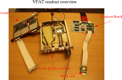
This page describes the GEM detector readout system. The system has four components, the VFAT readout card from CERN, a signal breakout box, a Gumstick I2C control computer, and an I/O VME module to record the LVDS output from the VFAT card.
Readout Scheme overview
| Module | Desc |
| [V1495] | An FPGA to source the MCLK and Trig signals as well as record the VFAT LVDS output. An external clock is used to drive the MCLCK pulse. |
| Power and I2C | A custom NIM module which houses a VFAT_readout_electronics#Power_supply and a VFAT_readout_electronics#Gumstick_I2C_controller used for I2C controls |
| Breakout board | A custom board used as a branch highway for both the LVDS and I2C signals to and from up to 6 VFAT cards. Warren Parson Thesis describing most of the system. |
| VFAT | VFAT readout Card |
New Parts Order List for Rev 4
20 1uF 805 Capacitors http://search.digikey.com/scripts/DkSearch/dksus.dll?Detail&name=490-1695-1-ND
20 80Ohm Common-mode filters http://search.digikey.com/scripts/DkSearch/dksus.dll?Detail&name=240-2475-1-ND
20 150Ohm Common-mode filters http://search.digikey.com/scripts/DkSearch/dksus.dll?Detail&name=240-2473-1-ND
(I'm not sure which of these will work best yet.)
5(ish) BNC Female Sockets http://search.digikey.com/scripts/DkSearch/dksus.dll?Detail&name=A32260-ND
10(ish) BNC Male Connectors http://search.digikey.com/scripts/DkSearch/dksus.dll?Detail&name=A24483-ND
(You might have a better idea for the BNC items, however.)
We also need larger-valued resistors for the LEDs on the board, but I'd have to look at the new circuit board again to get these values. I get this first thing tomorrow morning. (Unless Brian beats me to it.)
2 PES51 Soldiering Iron Tips...
1 of these http://search.digikey.com/scripts/DkSearch/dksus.dll?Detail&name=ETA-ND
And 1 of the slightly smaller version http://search.digikey.com/scripts/DkSearch/dksus.dll?Detail&name=ETH-ND
50 Jumpers: http://search.digikey.com/scripts/DkSearch/dksus.dll?Detail&name=3M9580-ND
VFAT readout Block Diagram
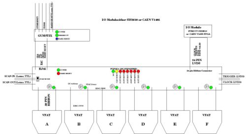
The diagram below describes the detector readout electronics for a GEM detector instrumented with 6 VFAT boards. Each VFAT board has 128 radout channels which are output through a single LVDS data line in series. A VFAT board from CERN is evaluated for use as a readout board to convert the GEM output analog signal to a digital signal.
RJ45 I2C + Power connector
| Pin | RJ45 Color Code | VFAT color Code/ Pin Number | Desc |
| 1 | white with orange spots | B25 | Analog Ground |
| 2 | solid orange | A25 | Analog Vcc |
| 3 | white with green | A7 | Hard Reset goes to +Vcc |
| 4 | solid blue | A2 | SCL |
| 5 | white with blue | B2 | SDA |
| 6 | green | not connected | |
| 7 | white with brown | B1 | Digital Ground |
| 8 | solid brown | A1 | Digital Vcc |
VFAT Board specifications
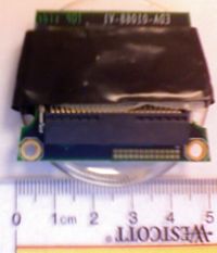
Photos of the top and bottom side of the VFAT card are shown below. The top side has a 50 pin connector which goes to the breakout box to separate I2C control signals and LVDS data I/O signals. The bottom side attaches to the GEM detector readout board via a 130 pin socket connector.
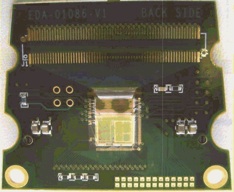
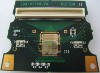
- 40 MHz sampling
- 128 channels
- can store up to 128 triggered events
- 0.25 m CMOS
- designed to withstand 100 MRad
- Single Event Upset protection using triple logic flip flops testable via a scan chain
- I2C control
- LVDS output
Signals
LVDS Signals to I/O module using 34 pin ribbon cable
National Semiconductor LVDS site
LVDS signals should be able to go 10 m
Media:Image:LVDS_EvaluationKit.pdf
[National Semiconductor suggests 15 m in section 2.5]
change to CAT 5 cable and you may be able to hit 80 m for 40 Mb/s
I2C signals
I2C (Can travel 8 m)
Let's try system for 150 ft transmission
I2C LED tester
The led.arm program turns the led a random color if run with no arguments, or you can specify r, g, b, or a combination of those, in the first argument:
./led.arm #random
./led.arm r #red
./led.arm rg #purple
Other things that could be tested are looking at the SDA/SCL signal on the vfat cable pulled apart on the breadboard, hooking the led light up to the breakout cable breadboard, or bypassing the breakout board i2c signals to the breadboard.
Breakout box specs (preliminary)
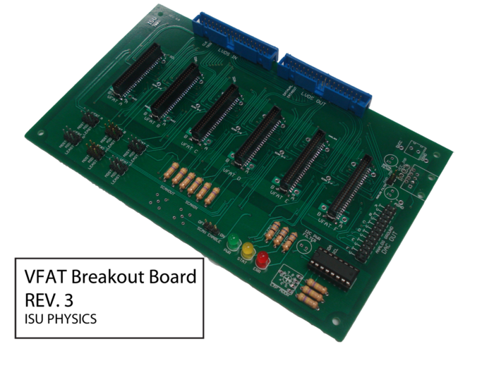
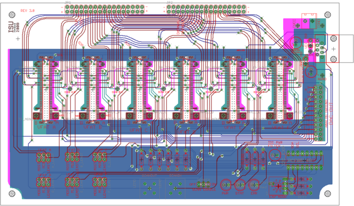
The breakoutbox is a circuit board with no active elements that separates the I2C command signal lines from the LVDS data I/O lines. The box is designed to support 6 VFAT readout cards. The box is being designed to be mounted on the detector rotator. All 6 VFAT cards will have their signal lines go into the break out box. The I2C lines will then go our of the breakout box along an RJ45 standard ethernet cable. The LVDS lines will exit though a standard 34 pin ribbon cable(Connector type Robinson Nugent P50E-068-P1-SR1-TG).
- 6 inputs for ~1m ribbon cables from VFAT modules
- 3-bit DIP switch to select I2C address range for each VFAT
- Soft reset for each VFAT controlled via I2C expander chip
- Shared hard reset line from Gumstix
- Scan Mode switch
- ScanIn connector (cascaded)
- ScanOut connector (cascaded)
- RJ45 port to gumstix box containing I2C and other signals:
- Power (3.3 or 2.5V)
- Ground
- SDA
- SCL
- Hard Reset
- Extra line for Link detection
- 34 pin ribbon connector for LVDS signals
- LEMO connector for LVDS trigger input
- LEMO connector for LVDS Master Clock
- I2C expander(s) for status LEDs (socketed)
- Status LEDs:
- Power (from I2C line)
- I2C connect (flashing through I2C expand)
- Power for each VFAT (feedback through common pins on VFAT board?)
- Hard Reset LED
- Clear UpsetReg (SEU counter) via I2C expand
Ribbon cable pinouts
The B side of the connector is the same side as the cable polarity notch.
| # | VFAT pin # |
Name | Value | Test rig color Primary/Second (Bigger color/smaller color) |
| B1 | DGND | Digital Ground | Black/Grey (shared) | |
| A1 | DVDD | +2.5V | Red/Grey (shared) | |
| B2 | 168 | SDA | I2C Data | Green/Yellow |
| A2 | 167 | SCL | I2C Clock | Yellow/Green |
| B3 | DGND | Digital Ground | Black/Grey (shared) | |
| A3 | DVDD | +2.5V | Red/Grey (shared) | |
| B4 | 162 | DACo-V | DAC output Volt | No Connection |
| A4 | 163 | DACo-I | DAC output Current | No Connection |
| B5 | 164 | I2C ADDR 2 | I2C Address Most | White/Blue |
| A5 | 165 | I2C ADDR 1 | I2C Address Middle | White/Orange |
| B6 | 166 | I2C ADDR 0 | I2C Address Least | White/Green |
| A6 | 169 | REsB | Soft Reset (Program saved) | White/Grey |
| B7 | 170 | ForceRehOff | ?? bond to grnd | No Connection |
| A7 | 171 | REhB | Hard Reset | Grey/White |
| B8 | 173 | MCLKB (-) | Orange/Purple | |
| A8 | 174 | MCLK (+) | Purple/Orange | |
| B9 | 175 | T1B (-) | Green/Purple | |
| A9 | 176 | T1 (+) | Purple/Green | |
| B10 | 177 | ScanOut | Brown/Purple | |
| A10 | 178 | ScanIn | Purple/Brown | |
| B11 | 180 | DataValidB (-) | Grey/Purple | |
| A11 | 181 | DavaValid (+) | Purple/Grey | |
| B12 | 182 | DataOutB (-) | Blue/Black | |
| A12 | 183 | DataOut (+) | Black/Blue | |
| B13 | 184 | SB8 (-) | Orange/Black | |
| A13 | 185 | S8 (+) | Black/Orange | |
| B14 | 186 | SB7 (-) | Green/Red | |
| A14 | 187 | S7 (+) | Red/Green | |
| B15 | 188 | SB6 (-) | Orange/Red | |
| A15 | 189 | S6 (+) | Red/Orange | |
| B16 | 190 | SB5 (-) | Blue/Red | |
| A16 | 191 | S5 (+) | Red/Blue | |
| B17 | 192 | SB4 (-) | Grey/Yellow | |
| A17 | 193 | S4 (+) | Yellow/Grey | |
| B18 | 194 | SB3 (-) | Brown/Yellow | |
| A18 | 195 | S3 (+) | Yellow/Brown | |
| B19 | 196 | SB2 (-) | Orange/Yellow | |
| A19 | 197 | S2 (+) | Yellow/Orange | |
| B20 | 198 | SB1 (-) | Blue/Yellow | |
| A20 | 199 | S1 (+) | Yellow/Blue | |
| B21 | DGND | Digital Ground | No Connection | |
| A21 | DVDD | +2.5V | No Connection | |
| B22 | DGND | Digital Ground | No Connection | |
| A22 | 179 | ScanEn | Scan Mode Enable | No Connection |
| B23 | AGND | Analog Ground | No Connection | |
| A23 | AVDD | 2.5V | Grey/Red | |
| B24 | AGND | Analog Ground | Grey/Black | |
| A24 | AVDD | 2.5V | Grey/Red | |
| B25 | AGNDD | Analog Ground | Grey/Black | |
| A25 | AVDD | 2.5V | Grey/Red |
The PC board-mount socket for the cable is ERNI 154765 for reel or ERNI 063197 for tube packaging.
The cable crimp-ons are ERNI 024403 or premade cables 300mm long are ERNI 173795
DF test Pattern
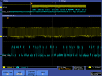
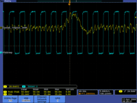
The VFAT board has a default test pattern it will send to DataOut. The pattern is shown in the figure to the right. To get the pulse you need to program the board using I2C commands to turn on the DFtestPattern bit the the extended control registers. Using our bitflip function this would correspond to bit 4 at the extended control register address 134. turning it on is done using the command
echo "e 112 134 0x10 set" | flipbit.arm
on the Gumstick controller
you turn it off with the command
echo "e 112 134 0x10 flip" | flipbit.arm
to the VFAT card at address 112.
Arduino
Gumstick I2C controller
Gumstix JLab addresses:
- gemgumstix.jlab.org
- MAC adresss HWaddr: 00:15:c9:0F:A5:D0
- IP = 129.57.36.61
- gemgumstix1.jlab.org
- MAC adress HWaddr: BA:53:FD:A3:7D:D1
- IP = 129.57.36.110
The gumstix motherboard used is the verdex XL6P. It has a 600MHz Marvell XScale processor, 128MB of RAM, and 32MB of flash.
More information: Gumstix
![]()
Web Interface
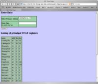
The I2C commands from the Gumstick to the VFAT board may be controlled through the web interface (if it is turned on)
Flipbit command interface
Once logged into the Gumstix, I2C registers on the VFAT can be modified using the flipbit interface. The flipbit.arm program takes input on standard input as shown in the following example:
echo p 41 2 on | flip bit
Field 1:
- "p" is for primary register.
- "e" is for extended register.
Field 2:
- if "p" i2c address of the register to be modified. Must be between 0 and 128 inclusive
- if "e" the value of the extended register to modify. Must be between 0 and 256 inclusive
Field 3:
- the bit (counting from 0=least significant) to modify. Must be between 0 and 7 inclusive
Field 4:
- "on" turn the bit on.
- "off" turn the bit off.
- "flip" flip the bit. (on if it was off, off if it was on)
Using standard input allows commands to be chained. The following example toggles bits 6 and 7 of address 64:
echo "p 64 7 flip p 64 6 flip" | flipbit.arm
If a # is used at the beginning of a line or after the standard arguments, the rest of the line is ignored. This is helpful when commands are stored in a file for later. Contents of an example cal.fb file:
#Turns on common calibration settings

#toggle calmode registers
p 64 6 flip #CalMode<0>
p 64 7 flip #CalMode<1>

#switch a few channels into calibration mode
e 2  7 on #channel 2
e 3  7 on #channel 3
Using that cal.fb file:
# flipbit.arm < cal.fb
Using mode p
Using address 64
Using bit 6
Using action flip

Using mode p
Using address 64
Using bit 7
Using action flip

Using mode e
Using address 2
Using bit 7
Using action on

Using mode e
Using address 3
Using bit 7
Using action on
Gumstick software
how to install operating system
how to install I2C modules
how to compile scripts (vfat.cgi, flipbit)
the flipbit program is compiled on cairo( 134.50.203.169) and then downloaded to the gumstick (http://134.50.3.175/vfat.html)
First you need to set the path on cairo
export PATH=$PATH:/home/brian/gumstix-buildroot_j/build_arm_nofpu/staging_dir/bin
Then the command below will compile my programs stored in the VFAT subdirectory.
arm-linux-g++ flipbit.cpp vfatregister.cpp vfati2c.cpp -o flipbit.arm
lsmod
check that I2C module is loaded
# lsmod
Module                  Size  Used by
i2c_dev                 5892  0
i2c_pxa                 7648  0
i2c_core               16848  2 i2c_dev,i2c_pxa
ipv6                  248416  14
af_packet              16872  0
ohci_hcd               19620  0
usbcore               113340  2 ohci_hcd
pxa2xx_cs               3044  1
pxa2xx_core            10368  1 pxa2xx_cs
pcmcia                 25064  0
pcmcia_core            30576  2 pxa2xx_core,pcmcia
firmware_class          7520  1 pcmcia
smc91x                 16104  0
mii                     4736  1 smc91x
gumstix_smc91x          2816  1 smc91x
unix                   22292  16
VFAT CGI script
I2C VFAT commands
reset_i2c
This will reset the I2C communications. You need to do this iff you unlpug VFATs and try to talk to them
run.arm
This will turn sleep blocking off (turn on the VFAT card)
stop.arm
This will turn sleep blocking ON (turn OFF the VFAT card). It is safe to unplug the card after this.
I/O VME modules
Struct SIS3610
V1495 FPGA
Parts List
Power supply
Acopian Model A07NX210
File:AcopianA07NX210SpecSheet.pdf
Readout TIming
Let me recast your question.
The V1495 receives a trigger pulse through the G1 Lemo connector at time T=T0. The V1495 uses this pulse to generate 3 LV1A pulses and sends them to the VFAT board via connector "C" which arrive at the VFAT board at time T=T0+T1. The VFAT sees the LV1A pulse and copies 128 readout channels to SRAM2 from SRAM1. The copy happens at time T=T0+T1-T3 where T3 is the latency time programmed into the VFAT. The Latency T3 lets us label the "in time" data for readout.
The VFAT outputs data with a header that contains a field know as the Bunch crossing number (BCN) that is a 12 bit counter which increments with every clock pulse. That means it can count 4096 pulses before starting over from zero. If we run at 40 MHz (10 MHz), then this number resets to zero every 102 (409) usec. The header also has an event number which counts the LV1A trigger pulses.
If the event rate is 1 kHz (1 msec). The BCN will reset at least 102 times before we readout an event. The BCN is useful if we have multiple coincidence events within 100 microseconds of eachother. The EN (event number) will label events to synchronize the trigger events with the other ROCs for Region 2 and 3.
References
Media:VFat2_manual_10-2008.pdf
File:VFAT2 TestProcedure.pdf VFAT test procedure written by P. Aspell in 2006
Media:VFAT2_P_Aspell_9-3-07.pdf: [ http://cdsweb.cern.ch/record/1069906 Topical Workshop on Electronics for Particle Physics, Prague, Czech Republic, 03 - 07 Sep 2007, pp.292-296] VFAT2 : A front-end system on chip providing fast trigger information, digitized data storage and formatting for the charge sensitive readout of multi-channel silicon and gas particle detectors.
Media:P_Aspell_VFATTestPlatform_9-15-08.pdf:Pauls Aspell talk at Topical Workshop on Electronics for Particle Physics, Naxos, Greece, 15 - 19 Sep 2008, pp.544-548, "The VFAT Production Test Platform for the TOTEM Experiment "
VFAT Panasonic to ERNI adapter board
An adapter board to allow a VFAT board to be used on the old 20 pin Erni connectors.
Inverntory
| Ser # | Address | Date last observed default test pattern |
| 00-23293-e0-0078 | eadc | |
| 00-23293-e0-0074 | 71aa |
