Difference between revisions of "TF EIM Chapt6"
| Line 98: | Line 98: | ||
But at high values of <math>I_D</math> the increase in temperature decreases <math>I_D</math>. | But at high values of <math>I_D</math> the increase in temperature decreases <math>I_D</math>. | ||
| + | |||
| + | This feature of the JFET allows you to chain several together for amplification such that if one starts to overheat it will amplify less. | ||
=MOSFET= | =MOSFET= | ||
Revision as of 03:32, 6 April 2011
Field Effect Transistors (FET, JFET, MOSFET)
Properties
FETs differ from the bipolar transistors in the las chapter in that the current from a FET is only due to the majority charge carriers in the semiconductor while bi-polar transistors current is produced from both carrier types; electron and hole.
- higher input impedance than bi-polar
- less gain than bi-polar
- better temperature stability
JFET
JFET Junction Field Effect Transistor
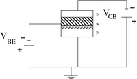
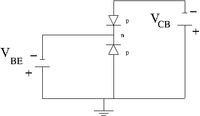
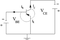
In a bi-polar transistor you have a depletion region with mixed charge carriers
 |
 |
|
| pnp bi-polar transistor | Equivalence circuit | Circuit diagram |
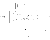
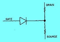
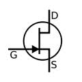
In the Junction Field Effect Transistor you have a single charge carrier with the minority charge carriers forming a choke point for the majority carrier current flow. It is similar to "pinching" a garden hose when water is flowing through it.
 |
 |
|
| JFET | Equivalence circuit | Circuit diagram |
The semiconductor material of the gate is the opposite of the channel. Here the n-p (or p-n) junction is between the gate and the channel.
The JFET operates by reverse biasing the gate-channel junction (diode) so the gate current doesn't flow in the direction indicated by the circuit diagram symbol. This means that the current through the gate is small (nAmps). As a result the input impedance looking into the gate is high (M) for the equivalent circuit.
The current junction rule is
for the Bi-Polar transistor
Resistance
The FET acts like a resistor.
Consider the following circuit
Let
the drain driving voltage
= resistor between the drain and V_{DD}
if = resistivity of the n-type semiconductor
then
- r = = resistance of the JFET
If you reverse bias the gate then the depletion region at the p-n junction expands into the n-type material thereby reducing the cross-sectional area (A) of the channel.
FET pinchoff
If you continue to reverse bias the gate, keeping V_{DD} constant, then the drain current will decrease as you make the gate more negative.
The pinchoff condition will occur when the reverse bias is large enough to stop the drain current I_D.
where
- = dielectric constant
- = thickness of the channel
- = number of impurity atoms per volume
You can find the "pinchoff" voltage by making V_{GS} more negative (n-channel) until the drain current I_D becomes zero.
In the other extreme
- Maximum drain current (current flows from Drain to Source with the gate Shorted; ie = 0)
Temperature
Because of the way a JFET operates, by pinching the current, the device heats up less at higher currents because you are no longer restricting the current flow.
At low values of and increase in the device temperature will cause an increase in .
But at high values of the increase in temperature decreases .
This feature of the JFET allows you to chain several together for amplification such that if one starts to overheat it will amplify less.
MOSFET
MOSFET Metal-Oxide-Semiconductor Field Effect Transistor