Difference between revisions of "TF EIM Chapt6"
Jump to navigation
Jump to search
(→JFET) |
(→JFET) |
||
| Line 18: | Line 18: | ||
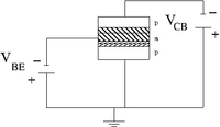
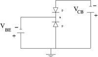
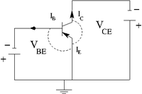
|[[File:TF_EIM_BipolarJunction.png| 200 px]] || [[File:TF_EIM_BipolarJunctionDiodeRep.png| 200 px]] ||[[File:TF_EIM_BipolarJunctionCircuit.png| 200 px]] | |[[File:TF_EIM_BipolarJunction.png| 200 px]] || [[File:TF_EIM_BipolarJunctionDiodeRep.png| 200 px]] ||[[File:TF_EIM_BipolarJunctionCircuit.png| 200 px]] | ||
|- | |- | ||
| − | | | + | | pnp bi-polar transistor || Equivalence circuit || Circuit diagram |
|- | |- | ||
|} | |} | ||
Revision as of 03:51, 4 April 2011
Field Effect Transistors (FET, JFET, MOSFET)
Properties
FETs differ from the bipolar transistors in the las chapter in that the current from a FET is only due to the majority charge carriers in the semiconductor while bi-polar transistors current is produced from both carrier types; electron and hole.
- higher input impedance than bi-polar
- less gain than bi-polar
JFET
JFET Junction Field Effect Transistor
 |
 |

|
| pnp bi-polar transistor | Equivalence circuit | Circuit diagram |
MOSFET
MOSFET Metal-Oxide-Semiconductor Field Effect Transistor