Difference between revisions of "HV-Circuit For TGEM-Detector"
Jump to navigation
Jump to search
| Line 17: | Line 17: | ||
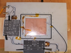
[[Image: HV_location.png | 250 px]] | [[Image: HV_location.png | 250 px]] | ||
| − | + | ||
[http://wiki.iac.isu.edu/index.php/Neutron_TGEM_Detector_Abdel#01.2F06.2F10_.28HV-circuit_Design.29 Go Back] | [http://wiki.iac.isu.edu/index.php/Neutron_TGEM_Detector_Abdel#01.2F06.2F10_.28HV-circuit_Design.29 Go Back] | ||
Revision as of 17:49, 2 June 2010
HV-Circuit Design
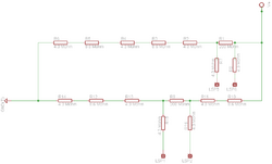
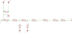
The HV- circuit for TGEM consists of two boards represented by the following schemes:
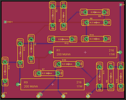
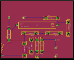
There are 10 cm X 8 cm boards, the 2nd board are deductible in size a little(instead of 8cm in width, it may reach 5cm), the following represent both of them with all the layers :
There is a little difference between the these schemes and the old ones that I added the filter for each board.
The location of the boards on the chamber:
