|
|
| (33 intermediate revisions by the same user not shown) |
| Line 7: |
Line 7: |
| | | 9/16/09 ||Finalize Committee | | | 9/16/09 ||Finalize Committee |
| | |- | | |- |
| − | | 9/25/09 || Stuff V3 Breakout Box | + | | 2/25/10 || Stuff V4 Breakout Box |
| | |- | | |- |
| − | | 10/2/09 || Schedule Prelim | + | |3/23/10 || Working Breakout Box |
| | |- | | |- |
| − | |10/23/09 || Working Breakout Box | + | | 5/20/2010|| S- curve automation |
| | |- | | |- |
| − | | 11/9/09 || S- curve automation | + | | 4/13/09 || Complete Draft of entire Thesis |
| | |- | | |- |
| − | | 9/13/09 || Final Draft of entire Thesis | + | | 4/23/10 || Make changes,Schedule Defense, and send copies to committee members (2 weeks to finish paperwork after defense) |
| − | |-
| |
| − | | 9/20/09 || Make changes,Schedule Defense, and send copies to committee members
| |
| | |} | | |} |
| | | | |
| − | =Thesis Chapters=
| |
| | | | |
| − | ==Abstract== | + | = Complete Thesis = |
| | | | |
| − | [[Abstract]] | + | [[File:MastersThesis.pdf]] |
| | | | |
| − | [[Media:Abstract.pdf]]
| + | = Required thesis changes= |
| | | | |
| − | ==Introduction==
| + | 1.) Add a conclusion |
| | | | |
| − | ==Chapter 1==
| + | 2.) work on description in pg 42 |
| | | | |
| − | == Chapter 2==
| + | 2.) Need S_curves and performance measurements. |
| | | | |
| − | =Detector description= | + | =Thesis Chapters= |
| | | | |
| − | ==Charge collector== | + | ==Abstract== |
| | | | |
| − | ==Output connector==
| + | [[Abstract]] |
| − | [[File:Qweak_R1_ChargeCollector_w_VFATLabels.png | 200 px]] | |
| | | | |
| − | == Strips - Output connector roadmap==
| + | [[Media:Abstract.pdf]] |
| − | A close up view of the 130 pin pads which will be used to mount connectors for the [[VFAT_readout_electronics]].
| |
| | | | |
| − | [https://panasonic-denko.co.jp/ac/e/control/connector/base-base/p5ks/number/index.jsp P5KS 130 pin 6.5 mm Panasonic connectors]
| + | ==Chapter 1 Introduction== |
| | | | |
| − | [https://panasonic-denko.co.jp/ac/e/control/connector/base-base/specdetail/index.jsp?part_no=AXK5SA3277YG Socket] | + | [[Introduction]] |
| | | | |
| − | [https://panasonic-denko.co.jp/ac/e/control/connector/base-base/specdetail/index.jsp?part_no=AXK6SA3677YG Header] | + | [[File:Introduction.pdf]] |
| | | | |
| − | [https://panasonic-denko.co.jp/ac/e_download/control/connector/base-base/catalog/con_eng_p5k.pdf SPEC sheet]
| + | ==Chapter 2 V1495 Module by CAEN== |
| | | | |
| − | We need to have plated holes which allow the copper lines to pass through to the very last layer where the copper pads for the 130 pin connector are.
| |
| − |
| |
| − |
| |
| − | [[Image:ConnectorPads.jpg | 500 px]]<br>
| |
| − |
| |
| − | ==VFAT==
| |
| − |
| |
| − | =Chapt V1495=
| |
| | [[V1495 Module by CAEN]] | | [[V1495 Module by CAEN]] |
| | | | |
| − | =Chapt Readout Controller=
| + | [[File:V1495 Module by CAEN.pdf]] |
| − | [[Readout Controller]] | |
| | | | |
| − | =Introduction= | + | ==Chapter 3 Readout Controller Library== |
| | | | |
| − | This thesis describes a system to digitally record the analog output of the Region 1 tracking system detectors used by the Qweak experiment at Jefferson Lab.
| + | [[Readout Controller Library]] |
| − | Analog electrical signals from the detector are processed by a preamplifier and a comparator integrated circuit developed by CERN as part of a front end electronics card referred to as the VFAT card<ref name="VFATcardRef"> VFAT card reference</ref>. The VFAT card includes a discriminator used to identify voltage levels which pass a value set through an I2C interface. The VFAT card<ref name="VFATcardRef" /> includes a digital to analog convert (DAC) which can be used to calibrate the card's circuitry on each of the 128 input channels. The VFAT card outputs a digital signal identifying which of the 128 channels received a charge beyond the preset threshold. The VFAT's digital signal is recorded using a field programmable gate array (FPGA) sold by CAEN as an input output module model number v1495.
| |
| | | | |
| − | The FPGA for the v1495 user firmware is a member of the Cyclone device family <ref>insert reference here for Cyclone family</ref>.
| + | [[File:Readout Controller Library.pdf]] |
| − | The complete operation and underpinnings of this device by itself are worthy of a separate thesis; the Cyclone Device Handbook, Volume 1, contains 385 pages. Of this, an understanding of perhaps 10 percent is sufficient to comprehend, operator, and effectively alter the properties of the Cyclone FPGA for the Region 1 detector.
| |
| | | | |
| − | Where necessary this thesis will reference and attempt to explain other portions from various manuals; all of these pertinent manuals are included on a CD with the original copy of this thesis. For the user firmware and the ROC (Read Out Controller) portions of the detector, UML diagrams have been included to simplify the process of familiarizing the reader with this detector and its respective algorithms for data acquisition from the VFATs. Unfortunately, due to the finite nature of this thesis there are many assumptions that are made about the level of technical proficiency of the reader; hopefully, these are minimal, but certainly they are unavoidable.
| + | ==Chapter 4 VFAT Breakout Board== |
| | | | |
| − | The Region 1 detector is comprised of the following individual systems and each one is described in its own section.
| + | [[VFAT Breakout Board]] |
| | | | |
| − | ;VFAT readout card
| + | [[File:VFAT Breakout Board.pdf]] |
| | | | |
| − | As paraphrased from the VFAT -- Operating Manual:
| + | ==Chapter 5 Conclusion== |
| | | | |
| − | The VFAT2 readout card is a trigger and front-end ASIC designed primarily for the TOTEM experiment. It has two basic functions: first, to gather fast regional hit information based on the creation of a charged pulse by an external event to one or more of the 128 VFAT channels; second, the FIFO data structures record and report the time and exact location per channel of the associated hit events for event post-processing.
| + | [[Conclusion]] |
| | | | |
| − | For the QWEAK Region 1 detector we do not utilize the first portion of the VFATs but instead use the charged pulse from a GEM detector to provide the trigger signal. The GEM detector system is discussed more thoroughly in the GEM Detector Section. However, we extensively use the second function of the VFAT detector.
| + | [[File:Conclusion.pdf]] |
| | | | |
| − | The VFAT detector can be described by a number of separate modules. These include the I2C communication, the preamp/filter/comparator modules, the T1 command interpreter, the FIFO hit report module including the associated data packing module, and the DAC for internal voltage and current sampling. Each one of these is described briefly, but here the reader is cautioned to read and understand the VFAT2 -- Operating Manual.
| + | ==Bibliography== |
| | | | |
| − | ;;I2C Communication Module
| + | [[Bibliography]] |
| | | | |
| − | ;Preamp/Filter/Comparator
| + | [[File:Bibliography.pdf]] |
| | | | |
| − | ;T1 Command Interpreter
| + | ==Appendix== |
| | | | |
| − | ;FIFO Hit Report Database
| + | [[Appendix]] |
| | | | |
| − | ;DAC
| + | [[File:Appendix.pdf]] |
| | | | |
| − | ;Gumstick
| + | ==Appendix== |
| | | | |
| | + | Do we want to include all of the source code and other various items in an appendix or do we want to simply include them in a CD along with the thesis? |
| | | | |
| | + | =Detector description= |
| | | | |
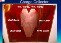
| | + | ==Charge collector== |
| | | | |
| − | [[V1495 Module by CAEN]] | + | ==Output connector== |
| | + | [[File:Qweak_R1_ChargeCollector_w_VFATLabels.png | 200 px]] |
| | | | |
| − | =V1495 Module by CAEN= | + | == Strips - Output connector roadmap== |
| | + | A close up view of the 130 pin pads which will be used to mount connectors for the [[VFAT_readout_electronics]]. |
| | | | |
| − | The final draft of this is ready to go. I will upload the text for this tomorrow in there respective sections.
| + | [https://panasonic-denko.co.jp/ac/e/control/connector/base-base/p5ks/number/index.jsp P5KS 130 pin 6.5 mm Panasonic connectors] |
| | | | |
| − | [[File:RoughDraft_V1495CAEN.pdf]] | + | [https://panasonic-denko.co.jp/ac/e/control/connector/base-base/specdetail/index.jsp?part_no=AXK5SA3277YG Socket] |
| | | | |
| | + | [https://panasonic-denko.co.jp/ac/e/control/connector/base-base/specdetail/index.jsp?part_no=AXK6SA3677YG Header] |
| | | | |
| | + | [https://panasonic-denko.co.jp/ac/e_download/control/connector/base-base/catalog/con_eng_p5k.pdf SPEC sheet] |
| | | | |
| − | Brief Overview of FPGAs
| + | We need to have plated holes which allow the copper lines to pass through to the very last layer where the copper pads for the 130 pin connector are. |
| | | | |
| − | FPGAs or “Field Programmable Gate Arrays” are electronic ICs -- typically digital -- that have the ability to be reprogrammed for different purposes. Quite often these circuits are used in the initial design phases of an IC when a hardwired circuit would be much more costly to produce for each revision of the product. Once the IC has been proven to work correctly, the design can then become hardwired onto an IC that can be mass produced.
| |
| | | | |
| − | In our experiment, we also use FPGAs for their ability to be reprogrammed, but we do not intend on mass-producing a hardwired version of our IC. We simply use its reprogrammable abilities to perform our highly specialized functionality. In this instance, we control the LVDS T1 signal going to the VFATs, extract the LVDS packets from the VFAT, store the data, and then pass it on to the ROC.
| + | [[Image:ConnectorPads.jpg | 500 px]]<br> |
| − | Brief Overview of HDL
| |
| | | | |
| − | When referring to electronics, HDL stands for “Hardware Description Language”. It is the term used for the code that describes hardware layout. For this reason it is also commonly referred to as “firmware” as it is neither completely software nor hardware. There are many different HDL languages, but the only two utilized for this project are VHDL (Very High Speed HDL) and Verilog. Most of the modules that the user will even want to change are those in VHDL; it is therefore recommended that if one wants to alter the user firmware for the v1495 that one spends most of one’s time learning VHDL. There is only one module in Verilog, v1495usr_hal.vqm: the purpose of which is described in its respective section.
| |
| | | | |
| − | HDL’s utility lies in its ability to describe hardware using a behavioral, a dataflow, or a structural model to describe the circuit one wants to build.
| |
| | | | |
| − | A behavioral model is one in which the user uses more traditional software flow-control statements to control the logical properties of the circuit; at this level in VHDL, these include “Process” statements, “If” statements, “Case” statements, Loop statements (e.g. “Do”, ”While”), “Next”/”Exit” statements, as well as “NULL” statements. It is at this level that the classic Mealy and Moore state machines are implemented.
| + | =Chapt V1495= |
| − | | + | [[V1495 Module by CAEN]] |
| − | Dataflow modeling is similar to behavioral modeling except instead of using flow-control similar to other traditional programs, one uses concurrent assignment operators to control the logical flow of data with operators such as “OR”, “AND”, “XOR”, etc. It has some conditional control like behavioral modeling, but it remains more low-level. It is conceivable that we could have used this form of modeling for the register-access modules, but these modules are in behavioral form of modeling.
| |
| − | | |
| − | Structural modeling is virtually a literal translation of traditional digital logic symbols (e.g. AND-gates, OR-gates, etc) into a software format. In structural modeling one uses previously-defined components to create the necessary logical operations by connecting their I/O’s properly. This form of modeling is very similar to Object Oriented Programming; the components can be thought of as the classes and the logical flow can be thought of as using the specific instantiations of the classes/components. For this thesis, we do not utilize this form of modeling either.
| |
| − | | |
| − | Bried Overview of Quartus II
| |
| − | Instructions for Downloading and running Quartus II
| |
| − | | |
| − | For this project we use the free Quartus II Web Edition Software. At the time of publication for this thesis, it is available at the following web address: http://www.altera.com/products/software/quartus-ii/web-edition/qts-we-index.html
| |
| − | | |
| − | Fortunately, for the purposes of this project, we only need to use it for its ability to handle and compile modules for the Cyclone family of FPGAs. It is, however, also useful for viewing the “Help” files on a number of modules in this project as well as viewing the pinouts for the FPGA (Assignments->Pins menu in Quartus). Although this level of detail is not necessary for this project, it does help one understand which signals are internal to the FPGA and therefore capable of being altered by the user firmware on the v1495, and which signals are external to the FPGA and not capable of being altered by the user firmware.
| |
| − | | |
| − | | |
| − | V1495_USR_firmware
| |
| − | | |
| − | Overview
| |
| − | | |
| − | The V1495_USR_firmware is provided by CAEN for the purpose of demonstrating how to use the v1495 module. This firmware as well as the is provided on the CD included with this thesis but can also be found on CAENs website. A number of functions are provided
| |
| − | GEMReadout Firmware
| |
| − | VHDL Modules
| |
| − | | |
| − | GEMReadout.vhd
| |
| − | | |
| − | This is the lowest hierarchical level for v1495 user firmware. It includes all of the I/Os as can be seen on the Pinout for the project. It also handles all of the receiving/transmitting functionality to/from the VFAT ICs, the FIFO storage, the PLL timing (if used), control of the LEDs on the v1495and the ROC interface capabilities.
| |
| − | | |
| − | As previously stated, it is not the intent of this thesis to clearly describe how VHDL works which is needed if one wants to be able to read the code to see how this module works but a UML
| |
| | | | |
| − | GEMTrigger.vhd
| |
| | | | |
| − | The GEMTrigger module handles the conversion of a single-pulse trigger to a 3-bit (or 8-bit in the case of the Calibration Pulse signal) trigger word which is sent to the T1 line of the VFATs which is in sync with the MCLK. The single-pulse trigger can be generated as a hard trigger from the G0 port, as a soft trigger internally, as a reset trigger internally, or even as a calibration trigger which can be generated either internally or externally depending on the value written to the A_GEM_CALIB_START register. Each of these triggers is more thoroughly described below.
| |
| − |
| |
| − | A hard trigger from the G0 input port when active generates whatever signal is located in HARD_TRIG_WORD. By default this is the LV1A signal, “100”, as this is probably used the most often. From the VFAT2 Manual we know that this is a request to the VFAT for a data packet of all of the hits on the lines. For a more thorough explanation of this process see the section in the VFAT2 Manual on page covering an LV1A request. HARD_TRIG_WORD is programmable by writing to bits 5-3 in register A_GEM_TRIG_WORD (offset + 0x0014). See Table (umptydump) for a list of the available registers on the v1495.
| |
| − |
| |
| − | A soft trigger is similar to a hard trigger except that is requested by a write operation to the A_GEM_SOFT_TRIG register. The SOFT_TRIGGER_WORD is located in bits 2-0 in register A_GEM_TRIG_WORD (offset + 0x0014). The default value for this word is “000”.
| |
| − |
| |
| − | The calibration trigger is the most complicated of all the triggers. Its main purpose is for quickly producing the S-curves necessary to adjust the threshold values for the channels on the VFATs high enough to reject systemic noise but still low enough to detect sensitive, real signals. A single sequence of the calibration trigger is comprised of a CalPulse signal , “110”, followed by a single blank clock cycle which is then followed by an LV1A signal, “100” to the T1 line.
| |
| − |
| |
| − | There are two different ways of using the calibration trigger pulse. A write to the A_GEM_CALIB_START (offset + 0x000E) register of 0x0000 – 0xFFFE (anything other than 0xFFFF) will cause a single burst of the calibration pulse sequence immediately following the write request. Writing 0xFFFF to this register causes the calibration pulse sequence to only pulse when a single external trigger pulse is applied to the G0 input. This can be done indefinitely and is changed by writing a value other than 0xFFFF to the aforementioned register. Originally it was intended to have the number being writing to this register control how many times the calibration pulse sequence was executed, but this functionality awaits future development.
| |
| − |
| |
| − | v1495usr_pkg.vhd
| |
| − |
| |
| − | This module simply contains the offset address for all of the user registers of the v1495. Table (umptydump), listed below, gives a detailed description of the names and addresses of these registers as listed in this module as well as their equivalent names in v1495Lib.o data structures.
| |
| − |
| |
| − | PLLBlock.vhd
| |
| − |
| |
| − | A PLL, Phase Lock Loop, is a timing stabilization mechanism. It is available to the users of the Cyclone for clock frequencies between 15Mhz and 1Ghz. At these extreme frequencies clock phase synchronization can become problematic for the internal hardware of the FPGA. By using at least one of the two available PLLs on the Cyclone FPGA, one can mitigate the clock phase synchronization error and thus achieve a much higher running frequency. For frequencies below 15Mhz the PLLBlock module is completely bypassed in the firmware. Usually these versions of the firmware include the suffix “NoPLL” in their names to indicate the difference.
| |
| − |
| |
| − | For the GEMReadout user firmware this module takes care to replicate the original MCLK signal coming in on G0 and outputting it to the PLLCLK signal (when referring to the VFAT is the MCLK). It also creates a clock signal that is an exact inverse of this signal. This signal has the misnomer PLLCLK_90. Since the VFATs change their output bits on a rising edge of MCLK and evaluate incoming bits on the falling edge of MCLK, the inputs and outputs to the v1495 are evaluated and changed on the rising edge of a clock 180 degrees out of phase with this (i.e. PLLCLK_90).
| |
| − |
| |
| − | The main portion of this module uses the “altpll” component from the Quartus II library. For a complete description of all of the attributes of this module see the help files in Quartus II on “altpll”. There are, however, a number of attributes that the user may need to change in order to run MCLK for the v1495 at a specific frequency between 15Mhz and 1Ghz. A listing and a brief description of each of these is provided below.
| |
| − |
| |
| − | inclk0_input_frequency: This is the value given for the frequency of the primary clock. The value is the period given in pico seconds and is not enclosed in quotations. This is not listed in the help-file literature. Example: A value of 25000 would give a primary running frequency of 40Mhz since 1/25000*10^-12 = 40Mhz
| |
| − |
| |
| − | clk1_phase_shift: This is the value given for the amount of phase shift on the secondary clock output relative to the primary clock output. This, too, is measured in picoseconds, but this attribute’s value does require quotations. Example: For the previous examples of 40Mhz, if the user requires a phase shift of 180 degrees the value of “12500” must be entered (i.e. half of the frequency period).
| |
| − |
| |
| − |
| |
| − | Verilog Modules
| |
| | | | |
| | =v1495usr.vhd= | | =v1495usr.vhd= |
| Line 269: |
Line 202: |
| | | | |
| | | | |
| − | ==ROC library==
| |
| − |
| |
| − | [[File:ReadoutController.pdf]]
| |
| | | | |
| − | [[Readout Controller]]
| |
| | | | |
| | ==Readout list== | | ==Readout list== |
| Line 306: |
Line 235: |
| | The "TRIGGER OUT" signal is used as the MCLK for the VFATs and "OUTPUT1" as the T1 signal for the VFAT. OUTPUT1 is set such that it will output the Calpulse signal followed by a single break pulse and then followed by the LV1A signal. The pattern is long enough that we should be able to see whether we received any hits on the lines that we have CalChan turned on in the respective ChanReg. Right now the experiment is running too quickly and does not have the proper setup to see whether the HitCount registers are working properly with the calibration pulses being sent. | | The "TRIGGER OUT" signal is used as the MCLK for the VFATs and "OUTPUT1" as the T1 signal for the VFAT. OUTPUT1 is set such that it will output the Calpulse signal followed by a single break pulse and then followed by the LV1A signal. The pattern is long enough that we should be able to see whether we received any hits on the lines that we have CalChan turned on in the respective ChanReg. Right now the experiment is running too quickly and does not have the proper setup to see whether the HitCount registers are working properly with the calibration pulses being sent. |
| | | | |
| − | =Breakout Board=
| |
| − |
| |
| − | The following section will describe the breakout board features as well as the design process.
| |
| | | | |
| | | | |
| | [http://wiki.iac.isu.edu/index.php/Warren_Parsons_Log_Book] [[Warren_Parsons_Log_Book]] | | [http://wiki.iac.isu.edu/index.php/Warren_Parsons_Log_Book] [[Warren_Parsons_Log_Book]] |
Warren_Parsons_Log_Book
| Date |
Task
|
| 9/16/09 |
Finalize Committee
|
| 2/25/10 |
Stuff V4 Breakout Box
|
| 3/23/10 |
Working Breakout Box
|
| 5/20/2010 |
S- curve automation
|
| 4/13/09 |
Complete Draft of entire Thesis
|
| 4/23/10 |
Make changes,Schedule Defense, and send copies to committee members (2 weeks to finish paperwork after defense)
|
Complete Thesis
File:MastersThesis.pdf
Required thesis changes
1.) Add a conclusion
2.) work on description in pg 42
2.) Need S_curves and performance measurements.
Thesis Chapters
Abstract
Abstract
Media:Abstract.pdf
Chapter 1 Introduction
Introduction
File:Introduction.pdf
Chapter 2 V1495 Module by CAEN
V1495 Module by CAEN
File:V1495 Module by CAEN.pdf
Chapter 3 Readout Controller Library
Readout Controller Library
File:Readout Controller Library.pdf
Chapter 4 VFAT Breakout Board
VFAT Breakout Board
File:VFAT Breakout Board.pdf
Chapter 5 Conclusion
Conclusion
File:Conclusion.pdf
Bibliography
Bibliography
File:Bibliography.pdf
Appendix
Appendix
File:Appendix.pdf
Appendix
Do we want to include all of the source code and other various items in an appendix or do we want to simply include them in a CD along with the thesis?
Detector description
Charge collector
Output connector
Strips - Output connector roadmap
A close up view of the 130 pin pads which will be used to mount connectors for the VFAT_readout_electronics.
P5KS 130 pin 6.5 mm Panasonic connectors
Socket
Header
SPEC sheet
We need to have plated holes which allow the copper lines to pass through to the very last layer where the copper pads for the 130 pin connector are.
Chapt V1495
V1495 Module by CAEN
v1495usr.vhd
- GEMReadout.vhd
The following is the UML for the GEMReadout module:
File:GEMReadoutUML.pdf
- GEMReadout_tb.vhd
- GEMRxChannel.vhd
The following is the UML for the GEMRxChannel module:
File:GEMRxChannelUML.pdf
- GEMRxEventDataFIFO.vhd
- a routine controlling the FIFO
- GEMRxEventSizeFIFO.vhd
- Defines the Event size and structure
- GEMTxChannel.vhd
The following is the UML for the GEMTxChannel module:
File:GEMTxChannelUML.pdf
- PLLVBlock.vhd
- spare_if_rtl.vhd
- tristate_if_trl.vhd
- v1495usr.vhd
- v1495usr_pkg.vhd
- GEMTrigger.vhd
The following is the UML diagram for the GEMTrigger module:
File:GEMTriggerUML.pdf
- v1495usr_hal.vqm
- From the v1495 manual this is the v1495 Hardware Abstraction Layer. It is an HDL module provided in Verilog format at the netlist level in order to help interface the hardware.
- Reading through this file makes it clear that we are using the Cyclone chip family. I can't find where the "cyclone_lcell" module is defined. I am wondering if it is defined inside of the Quartus II program in a library somewhere. Figuring this out would probably help unravel how our HDL code is actually instantiated in hardware.
General introduction to the readout scheme
Readout Blockdiagram
Changing MCLK frequency
Output MCLK and Level 1 Trigger
VFAT input port
V1495 Data format
CODA Readout
The V1495 module transfers data 16 bits at a time to the ROC. An array within the ROC memory will be filled with the V1495 data stream 16 bits at a time to optimize data throughout. The array within the ROC memory will then be transferred to the host computer and stored.
Move the source code to an appendix
File:V1495Lib.c
File:V1495Lib.h
File:V1495.c
File:V1495.h
File:V1495ReadoutCtrl.c
File:V1495ReadoutCtrl.h
File:GEMReadoutCtrl.c
File:GEMReadoutCtrl.h
File:Makefile.txt
Readout list
CODA Data Format
QwAnalaysis
Qweak_R1_Software
Calibration Pulse Experiment and Results
The following are the parameters that were used for the Calibration Pulse experiment.
MCLK = 40Mhz
IPreampIn 0xa8
IPreampFeed 0x50
IPreampOut 0x96
IShaper 0x96
IShaperFeed 0x64
IComp 0x78
MSPulseLength<2:0> = 0x0 // MonoStable pulse length of 1 clock period
HitCountSel<3:0> = 0x0 // Fast-OR of all 128 channels
The MCLK frequency was chosen because it is at which the original Calibration pulse experiments were run. Also, in the experiment the CalPulse signal supposedly has a peaking time of 22ns. Thus, if we want to have any hope of catching the calibration pulse, we will most likely need to run at at least 40 Mhz. This, of course, also depends on the peak amplitude of the pulse as well as how long its tail is.
The v1495 firmware performs a straight pass-through of the trigger signal from the pattern generator. Care has been taken to make sure that the signals are passed along while they are stable rather than at a transition. Also, it is known that the MCLK shown in Figure 10 of the VFAT manual is out of phase by 180o, thus care has also been taken to make sure that the T1 signal has the proper phase with respect to MCLK. This whole process causes the signal being output to be one clock cycle behind the signal being injected; this shouldn't be a problem.
The "TRIGGER OUT" signal is used as the MCLK for the VFATs and "OUTPUT1" as the T1 signal for the VFAT. OUTPUT1 is set such that it will output the Calpulse signal followed by a single break pulse and then followed by the LV1A signal. The pattern is long enough that we should be able to see whether we received any hits on the lines that we have CalChan turned on in the respective ChanReg. Right now the experiment is running too quickly and does not have the proper setup to see whether the HitCount registers are working properly with the calibration pulses being sent.
[1] Warren_Parsons_Log_Book

