Warren Parsons Log Book
This tracks My Daily Progress developing the VFAT readout
VHDL files for v1495
- GEMReadout.vhd
- The main function routines?
- GEMReadout_tb.vhd
- GEMRxChannel.vhd
- GEMRxEventDataFIFO.vhd
- a routine controlling the FIFO
- GEMRxEventSizeFIFO.vhd
- Defines the Event size and structure
- GEMTxChannel.vhd
- PLLVBlock.vhd
- spare_if_rtl.vhd
- tristate_if_trl.vhd
- v1495usr.vhd
- v1495usr_pkg.vhd
- v1495usr_hal.vqm
- From the v1495 manual this is the v1495 Hardware Abstraction Layer. It is an HDL module provided in Verilog format at the netlist level in order to help interface the hardware.
- Reading through this file makes it clear that we are using the Cyclone chip family. I can't find where the "cyclone_lcell" module is defined. I am wondering if it is defined inside of the Quartus II program in a library somewhere. Figuring this out would probably help unravel how our HDL code is actually instantiated in hardware.
5/14/09
Firmware
Today we started looking at the VHDL firmware programs from Ben Raydo at JLab. Our goal: To determine what the general description of the firmware program is and determine an outline of its functionality.
Quartus II
Quartus II has a fairly good tutorial for usage. My goal is to complete this tutorial by the end of the week.
I also started to familiarize myself with the VHDL programming language.
5/15/09
Spent vast majority of day learning VHDL syntax.
Spent some time reviewing the GEM Readout Controller Firmware Status
Spent some time reviewing the v1495 instruction manual ( the Quartus II instructions in particular )
Spent some time reviewing the VFAT instruction manual
- Is there a primer somewhere on how to communicate via/with VME?
- How about this http://www.vita.com/vmefaq.html
I need to write down how to get into the DAQ as well as ROC xterm windows.
- Tamuna can show you the above
5/18/09
- From the manual on the VFAT2
- Are we using the Roman Pots or the GEM version for the channel assignments? (I assume the latter.)
GEM version
If I understand the underlying functionality of the output of the VFAT2 then the basic idea is that it transfers the hit data from SRAM1 to SRAM2 as soon as there is a LV1A signal (100) sent to the VFAT2 via the "T1" line (after the latency time programmed into the Latency Register with a default setting of 6.4us).
I thought the max latency is 6.4 us and the default is zero
Once data is transferred from SRAM1 to SRAM2 it immediately starts outputing the information on "DataOut" at the "MCLK" rate of 40Mhz (I assume to be ultimately governed by the v1495). Valid data can be found on the "DataOut" line as long as the "DataValid" line is high. Thus the LV1A signal on "T1" followed by a transition to high on the "DataValid" line should set off the v1495 data capturing routine. Data is clocked out in FIFO order if more LV1A signals are sent to the VFAT2 before all of the data has been transferred out of the VFAT2.
I am unclear if the V1495 firmware is programmed to begin a read when the L1 trigger transitions or when DataValid transition. I think it should be when DataValid transitions.
Tamuna and I tried to log onto the ROC from scratch, but the ROC keeps saying that it can't find some boot file. I started to look through the ROC file on Dr. Forest's wiki pages, but I do not find this to be a straightforward process of rebooting the ROC. The following entry is related, and it may be helpful.
- Would it be useful to purchase the VMEbus Handbook, 4th Edition by Wade Peterson? I have personally never worked with such a complicated system with so few written resources as the VME system. I have now read quite a bit about the history of the VME system, and yet I have yet to be able to read anything on how to actually use this system. How does one begin to even crack into this system? It is a full-blown microcontroller complete with its own operating system including the complete gamut of hardware and software.
- Where did we get this Quartus II software from and why has the 30-day trial period run out? This may be making it so I cannot compile a project and get it loaded into the v1495 via the ROC. I get this impression from the fact that when I attempt to compile the project only one error comes up and that is that the 30-day evaluation period has expired. Do we have a license for it somewhere?
Licenses are free. see http://wiki.iac.isu.edu/index.php/Qweak_V1495_FPGA_Programming for the download page
5/19/09
Tamuna, Brian, and I worked on trying to fix the MVME6100 but to no avail. I think it's actually getting worse the more we try to get it working. We may need to wait until Dr. Forest returns before attempting to fix it. I plan on reading some more information that I found on the whole VME system as well as the MVME6100 and its associated OS, VXWorks, which is apparently used in a lot more applications than I was previously aware.
I was able to contact Ben Raydo. Thankfully he had given me quite a few suggestions on how to get started with the v1495 side of this project. I am sifting through the information he has given me.
I have found much more information on the VME system today including information on the MVME6100 (as already stated) as well as other documentation.
5/20/09
I had to brush up a bit on Verilog to figure out what was going on in the v1495usr_hal.vqm file because it is written in Verilog HDL. I have added its description above.
By whatever mystical powers the ROC is apparently now working again. I would however like to know exactly what happened to get it working.
I still need a license for Quartus II in order to continue working directly on the v1495. However, I did spend a great deal of time reading how to use the MVME6100 as well as the v1495.
5/21/09
I was able to figure out how to get the license for Quartus II and to compile an .rgb file that can be loaded into the v1495 USER FPGA. I was not aware before that we already had a completely working firmware version for the v1495 USER FPGA.
- In looking through the VHDL code to figure out how it works I have made the following discoveries
- The code in GEMReadout.vhd governs the behavior of the GEMReadout component.
- Code governing the G0 (Gin(0)) and G1 (Gin(1)) Inputs
- In GEMReadout.vhd the signal GIN(1) gets loaded into HARD_TRIGGER. HARD_TRIGGER then gets loaded into the HARD_TRIGGER of the GEMTrigger component as well as the HARD_TRIGGER of a GEMTxChannel component. Thus far I am unclear what is done with this HARD_TRIGGER signal for these components. I will figure this out on Friday, hopefully.
- Still in GEMReadout.vhd the GIN(0) signal gets loaded into the inclk0 value of the PLLBlock component. In PLLBlock.vhd (which governs the behavior of the PLLBlock component), this c0 signal eventually ends up being connected to clk(0) for the altpll component. The altpll component appears to be a predefined cell in Quartus II. I hypothesize that this component is just a pll with user-defined settings. Hopefully on Friday I can find some documentation on this component to figure out exactly how it works. Thus in GEMReadout.vhd we put in our original signal G0 and get out a locked version on PLLCLK.
- This appears to be in GEMReadout.vhd where the process trigger PLLCLK is generated. All other components that take this value in on one of its ports has it as an input rather than an output.
- nLBRES is a system-wide asyncronous reset
- LCKL is a local bus clock
- I cannot figure out where this is being generated because I lose its trail into the v1495usr_hal.vqm file going to
5/22/09
altpll is indeed an Altera Megafunction. inclk0 is the reference clock to the output clocks c0 and c1. c0 is exactly in phase with inclk0 which appears to be running at a nominal frequency of 32Mhz which as stated before ultimately ends up being the PLLCLK signal in the GEMReadout block. c1 is a phase shifted version of inclk0. Although it states that this ends up being PLLCLK_90 in GEMReadout.vhd, it is actually 180 of phase shift, i.e. an inverted clock pulse. I don't know why it was given this name since it doesn't make sense.
These calculation can be done using the input parameters to the altpll plock in the PLLBlock.vhd code from the following lines.
altpll_component : altpll GENERIC MAP (
- clk0_divide_by => 1,
- clk0_duty_cycle => 50,
- clk0_multiply_by => 1,
- clk0_phase_shift => "0",
- clk1_divide_by => 1,
- clk1_duty_cycle => 50,
- clk1_multiply_by => 1,
- ;clk1_phase_shift => "15625", <-- This is the phase shift in ps.
- compensate_clock => "CLK0",
- ;inclk0_input_frequency => 31250, <-- This is the input frequency given as the period in ps.
- intended_device_family => "Cyclone",
- invalid_lock_multiplier => 5,
- lpm_hint => "CBX_MODULE_PREFIX=PLLBlock",
- lpm_type => "altpll",
- operation_mode => "NORMAL",
The units for the frequency cannot be found in the literature. The way I figured this out was to create an altpll Megafunction block with a strange frequency. After it generated the VHDL code for the megafunction I was able to see that the output of the inclk0_input_frequency was in ps.
5/26/09
- On the question of I/O Levels.
- There are two different pin voltage levels to consider here: the I/O levels coming into the board and the I/O levels of the Cyclone chip.
- The input levels going into G0 and G1 are LVTTL (3.3V). This information, as well as the pin output assignments, are located under the menu "Assignments->Pins" in the Quartus II program.
- This information is part of the project that was created for this design. What that means is that it is not enough to just import the text files for this project and compile it. One needs the project file ".qfp" which has all of the proper pin assignments including location and levels.
- The I/O levels going into and out of the v1495 is much more difficult to ascertain. The following is an example from the GEMReadout.vhd file which programs the levels as well as whether a pin is input or output.
- The nOEx signals are whether or not a bidirectional pin is configured as an output or an input. A logic level "0" is an input.
- The SELG signals are whether or not a pin is TTL or NIM on the G I/Os. A logic level "0" indicates that this is a TTL level.
- The preceeding was gleaned from the v1495usr_demo project that can be downloaded for free from CAEN. There must be some hardware external to the Cyclone chip but still on the v1495 that selects these settings.
- Thus far I have not found the documentation that demostrates how this is actually done. Like I said before, at this point I have only been able to glean the information from the v1495user_demo project. Therefore, it would not surprise me if this information was somewhat faulty.
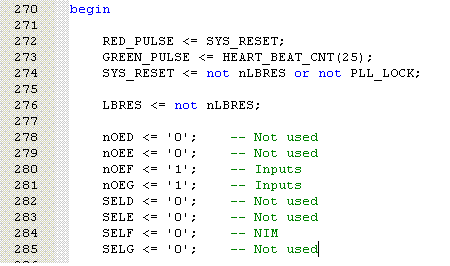
The following code was used to see if I could turn off the Red LED:
RED_PULSE <= SYS_RESET;
GREEN_PULSE <= HEART_BEAT_CNT(25);
-- SYS_RESET <= not nLBRES or not PLL_LOCK;
After resetting the VME crate, it appears to have worked. I was previously under the impression that one did not have to bump the power on the v1495 to get it to use its new firmware. I will have to explore this.
The rate at which the Green LED blinks is based off of the following code out of GEMReadout.vhd.
signal HEART_BEAT_CNT : std_logic_vector(25 downto 0);
process(LCLK, nLBRES)
 begin
  if nLBRES = '0' then
   HEART_BEAT_CNT <= (others => '0');
  elsif rising_edge(LCLK) then
   HEART_BEAT_CNT <= HEART_BEAT_CNT + 1;
  end if;
end process;
Basically what these lines of code are saying is that HEART_BEAT_CNT is a 26-bit register that originally gets set to '0'. On either a change in LCLK or nLBRES and if LCLK is a rising edge, then the HEART_BEAT_CNT gets incremented by one. From the lines of code shown before this block, GREEN_PULSE is set if the MSB of HEART_BEAT_CNT is set. Therefore, the Green LED should blink at a 50% duty cycle of 2^(25)*(20Mhz)^(-1) = 3.35 s for a 20MHz PLL frequency (i.e. on for 1.67s, off for 1.67 s).
Tomorrow I will need to determine what the signals "SYS_RESET, nLBRES, and PLL_LOCK" actually are and what they mean. As I have alluded to before, I loose the trail for many of these signals at the Cyclone package level and can only infer what their actual purposes are at this point based on the code from the GEMReadout as well as the v1495usr_demo.
5/27/09
I then doubled the PLL frequency to see if it would double the rate at which the LED was blinking. It worked.
- What this means is that the LCLK signal is somehow internal to the chip and has nothing to do with the signal that is being injected on G0.
I then changed the code back on the RED LED to see if I could restore the RED LED status with the new faster GREEN LED rate.
- This worked as well.
I attempted to change the firmware back to the original 20MHz configuration, but it does not seem to have slowed down the blinking GREEN LED at all. I am wondering if the 20MHz version was somehow corrupted. I will recompile and send this over to see if I can slow the blinking GREEN LED down.
 Note: This is because the Green LED depends on the system "LCLK" rather
than the "PLLCLK" which is supposed to be a reflected version of the G0 input.
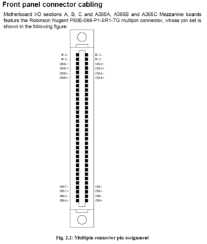
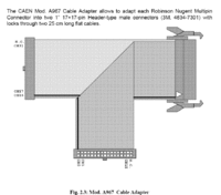
The following multipin connector settings can be found in the v1495 user manual and show explicitly where the proper pin connections can be made.
For my last item of the day I attempted to reset the Green LED to blink with "PLLCLK" rather than "LCLK." This only led to the Green LED remaining solid. This, as well as our previously failed attempts to lock with the frequency of the PLL, seems to suggest that the v1495 is not even registering the G0 input.
5/28/09
Today I attempted to get the LED to blink to the LCLK rather than the PLLCLK. It did not work.
Later I attempted to get C(1) to output the LCLK, which drives the Green LED, rather than PLLCLK_90. This also did not work.
Both of these seem to suggest that the Cyclone chip is somehow to communicating to the I/O ports on the v1495.
5/29/09
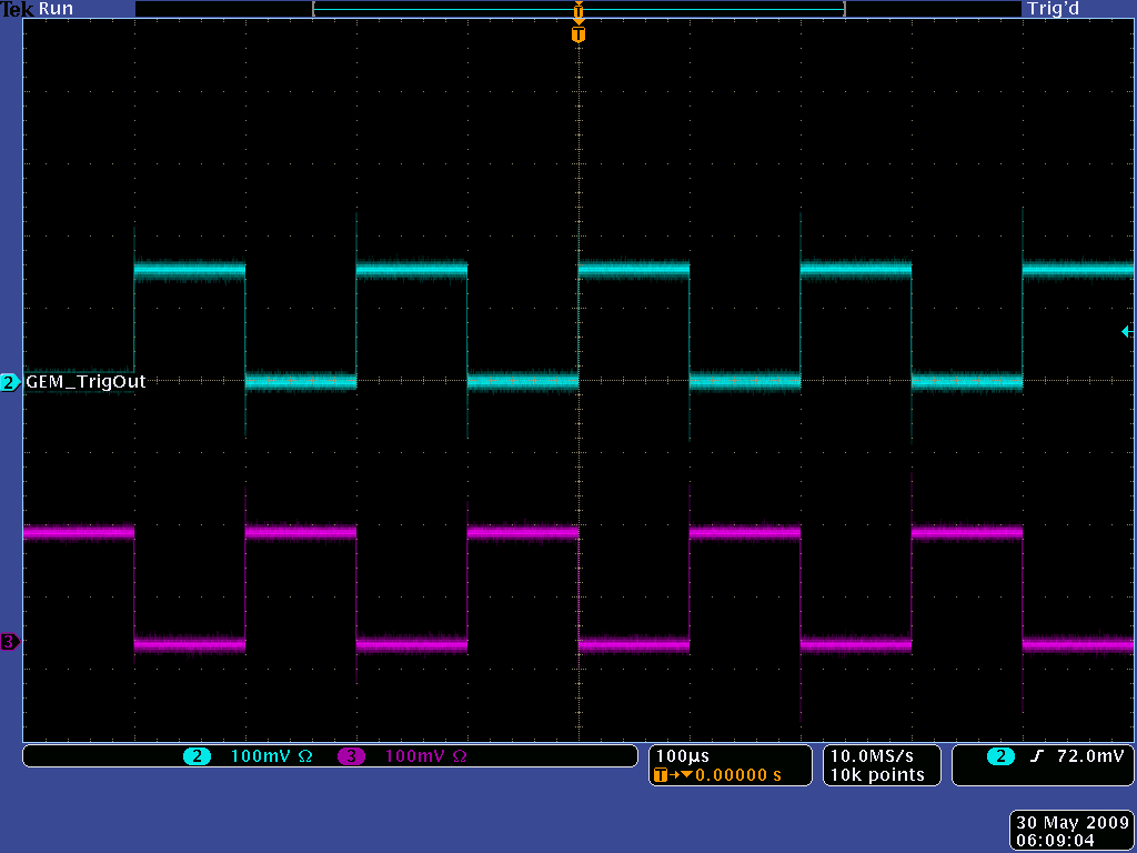
On the output of the oscilloscope below, Line2 is the output from C(3) and Line3 is the output from C(5).


