Difference between revisions of "VFAT readout electronics"
| Line 6: | Line 6: | ||
A VFAT board from CERN is evaluated for use as a readout board to convert the GEM output analog signal to a digital signal. | A VFAT board from CERN is evaluated for use as a readout board to convert the GEM output analog signal to a digital signal. | ||
| − | <center>[[Image:BreakOutBox.jpg | 400 px]][[Media:BreakOutBox.text]] | + | <center>[[Image:BreakOutBox.jpg | 400 px]]</center><br>[[Media:BreakOutBox.text]] |
<br> | <br> | ||
<br> | <br> | ||
Revision as of 11:51, 28 July 2008
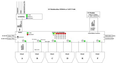
This page describes the GEM detector readout system for the Qweak experiment. The system has four components, the VFAT readout card from CERN, a signal breakout box, a Gumstick I2C control computer, and an I/O VME module to record the LVDS output from the VFAT card.
VFAT readout Block Diagram
The diagram below describes the detector readout electronics for a GEM detector instrumented with 6 VFAT boards. Each VFAT board has 128 radout channels which are output through a single LVDS data line in series. A VFAT board from CERN is evaluated for use as a readout board to convert the GEM output analog signal to a digital signal.
Target View:
- Dimensions:
- Width: 7.5"
- Height: 4.5"
VFAT Board specifications
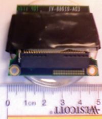
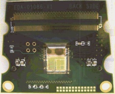
Photos of the top and bottom side of the VFAT card are shown below. The top side has a 50 pin connector which goes to the breakout box to separate I2C control signals and LVDS data I/O signals. The bottom side attaches to the GEM detector readout board via a 130 pin header connector.
- 40 MHz sampling
- 128 channels
- can store up to 128 triggered events
- 0.25 m CMOS
- designed to withstand 100 MRad
- Single Event Upset protection using triple logic flip flops testable via a scan chain
- I2C control
- LVDS output
Signals
LVDS Signals to I/O module using 34 pin ribbon cable
LVDS
LVDS signals should be able to go 10 m
I2C signals
I2C (Can travel 8 m)
Breakout box specs (preliminary)
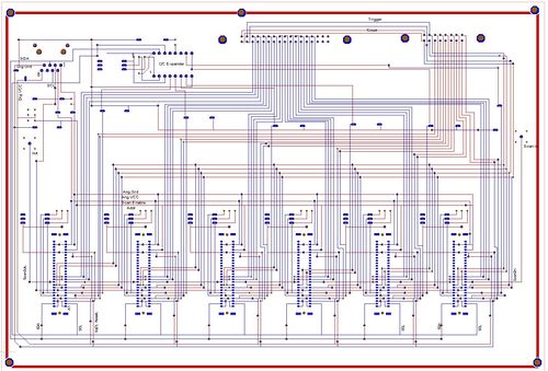
The breakoutbox is a circuit board with no active elements that separates the I2C command signal lines from the LVDS data I/O lines. The box is designed to support 6 VFAT readout cards. The box is being design to be mounted on the detector rotator. All 6 VFAT cards will have their signal lines go into the break out box. The I2C lines will then go our of the breakout box along an RJ45 standard ethernet cable. The LVDS lines will exit though a standard 34 pin ribbon cable(Connector type Robinson Nugent P50E-068-P1-SR1-TG).
- 6 inputs for ~1m ribbon cables from VFAT modules
- 3-bit DIP switch to select I2C address range for each VFAT
- Soft reset for each VFAT controlled via I2C expander chip
- Shared hard reset line from Gumstix
- Scan Mode switch
- ScanIn connector (cascaded)
- ScanOut connector (cascaded)
- RJ45 port to gumstix box containing I2C and other signals:
- Power (3.3 or 2.5V)
- Ground
- SDA
- SCL
- Hard Reset
- Extra line for Link detection
- 34 pin ribbon connector for LVDS signals
- LEMO connector for LVDS trigger input
- LEMO connector for LVDS Master Clock
- I2C expander(s) for status LEDs (socketed)
- Status LEDs:
- Power (from I2C line)
- I2C connect (flashing through I2C expand)
- Power for each VFAT (feedback through common pins on VFAT board?)
- Hard Reset LED
- Clear UpsetReg (SEU counter) via I2C expand
Ribbon cable pinouts
| # | VFAT pin # |
Name | Value | Test rig color Primary/Second |
| B1 | DGND | Digital Ground | Black/Grey (shared) | |
| A1 | DVDD | +2.5V | Red/Grey (shared) | |
| B2 | 168 | SDA | I2C Data | Green/Yellow |
| A2 | 167 | SCL | I2C Clock | Yellow/Green |
| B3 | DGND | Digital Ground | Black/Grey (shared) | |
| A3 | DVDD | +2.5V | Red/Grey (shared) | |
| B4 | 162 | DACo-V | DAC output Volt | |
| A4 | 163 | DACo-I | DAC output Current | |
| B5 | 164 | I2C ADDR 2 | I2C Address Most | White/Blue |
| A5 | 165 | I2C ADDR 1 | I2C Address Middle | White/Orange |
| B6 | 166 | I2C ADDR 0 | I2C Address Least | White/Green |
| A6 | 169 | REsB | Soft Reset (Program saved) | White/Grey |
| B7 | 170 | ForceRehOff | ?? bond to grnd | |
| A7 | 171 | REhB | Hard Reset | Grey/White |
| B8 | 173 | MCLKB (-) | ||
| A8 | 174 | MCLK (+) | ||
| B9 | 175 | T1B (-) | ||
| A9 | 176 | T1 (+) | ||
| B10 | 177 | ScanOut | ||
| A10 | 178 | ScanIn | ||
| B11 | 180 | DataValidB (-) | ||
| A11 | 181 | DavaValid (+) | ||
| B12 | 182 | DataOutB (-) | ||
| A12 | 183 | DataOut (+) | ||
| B13 | 184 | SB8 (-) | ||
| A13 | 185 | S8 (+) | ||
| B14 | 186 | SB7 (-) | ||
| A14 | 187 | S7 (+) | ||
| B15 | 188 | SB6 (-) | ||
| A15 | 189 | S6 (+) | ||
| B16 | 190 | SB5 (-) | ||
| A16 | 191 | S5 (+) | ||
| B17 | 192 | SB4 (-) | ||
| A17 | 193 | S4 (+) | ||
| B18 | 194 | SB3 (-) | ||
| A18 | 195 | S3 (+) | ||
| B19 | 196 | SB2 (-) | ||
| A19 | 197 | S2 (+) | ||
| B20 | 198 | SB1 (-) | ||
| A20 | 199 | S1 (+) | ||
| B21 | DGND | Digital Ground | ||
| A21 | DVDD | +2.5V | ||
| B22 | DGND | Digital Ground | ||
| A22 | 179 | ScanEn | Scan Mode Enable | |
| B23 | AGND | Analog Ground | ||
| A23 | AVDD | 2.5V | Grey/Red | |
| B24 | AGND | Analog Ground | ||
| A24 | AVDD | 2.5V | Grey/Red | |
| B25 | AGNDD | Analog Ground?? | Grey/Black | |
| A25 | AVDD | 2.5V | Grey/Red |
The PC board-mount socket for the cable is ERNI 154765 for reel or ERNI 063197 for tube packaging.
The cable crimp-ons are ERNI 024403 or premade cables 300mm long are ERNI 173795
Gumstick I2C controller
The gumstix motherboard used is the verdex XL6P. It has a 600MHz Marvell XScale processor, 128MB of RAM, and 32MB of flash.
More information: Gumstix
![]()
Web Interface
The I2C commands from the Gumstick to the VFAT board may be controlled through the web interface (if it is turned on)
