Difference between revisions of "TamarD Logbook"
| Line 623: | Line 623: | ||
[[Image:Amplified_pulse_from_PMT_11013Volts_2-12-08.png|200px]][[Image:Amplified_pulse_from_PMT_and_Discriminator_1013Volts_2-12-08.png|200px]]<br> | [[Image:Amplified_pulse_from_PMT_11013Volts_2-12-08.png|200px]][[Image:Amplified_pulse_from_PMT_and_Discriminator_1013Volts_2-12-08.png|200px]]<br> | ||
| + | |||
| + | |||
| + | -> c775PrintEvent | ||
| + | TDC DATA for Module 0 | ||
| + | Header: 0xfa001000 nWords = 16 | ||
| + | 0xf8004252 0xf80140e9 0xf80240d3 0xf80340e5 0xf80440e5 | ||
| + | 0xf80540f4 0xf80640ef 0xf807418a 0xf8084195 0xf80942d9 | ||
| + | 0xf80a418b 0xf80b4184 0xf80c4140 0xf80d413d 0xf80e4152 | ||
| + | 0xf80f414d | ||
| + | Trailer: 0xfc000000 Event Count = 0 | ||
| + | value = 18 = 0x12 | ||
| + | -> c775PrintEvent | ||
| + | TDC DATA for Module 0 | ||
| + | Header: 0xfa001000 nWords = 16 | ||
| + | 0xf8004214 0xf8014172 0xf802415a 0xf80340af 0xf804416e | ||
| + | 0xf805417a 0xf806424a 0xf80740b5 0xf80841a5 0xf809419a | ||
| + | 0xf80a40b9 0xf80b4195 0xf80c418e 0xf80d40b2 0xf80e4193 | ||
| + | 0xf80f4184 | ||
| + | Trailer: 0xfc000001 Event Count = 1 | ||
| + | value = 18 = 0x12 | ||
| + | |||
| + | |||
[http://www.iac.isu.edu/mediawiki/index.php/Delta_D_over_D Go Back] | [http://www.iac.isu.edu/mediawiki/index.php/Delta_D_over_D Go Back] | ||
Revision as of 02:46, 3 December 2008
9/5/08
Detector Construction
4 chambers are built.
TGEM:
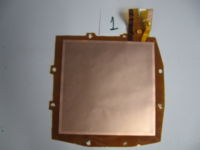
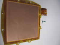
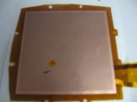
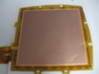
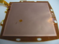
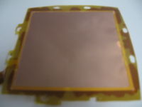
Foils have been mounted on the TGEM comparison chamber. Both charge collectors are mounted on the TGEM test detectors. One TGEM test detector has the Thick PC board GEM foils which need much higher HV than the regular GEM foils. The second TGEM test chamber has 3 GEM foils from CERN.
Need a min of 32 1 Meg Ohm resistors to complete the output termination connectors. Need 32 more termination connectors made from 16 wires.
Need to grind down 16, M3 bolts for mounting the GEM foils and TGEM PCboards.
Need 24 washers for GEM foils. Check mounting of the TGEM boards. Look up spacing and HV for the TGEM boards[1], Media:01352098.pdf .
Need to etch 2 cathodes for the TGEm boards.
Qweak:
a.) Need to do final outer footprint machining so there is no interference with the Electron profile of the other octant.
b.) Need to machining back of the chamber for the Charge collector
c.) Need to machine thick frames for the cathode and maybe GEM foils.
d.) Apply electrical insulation to HV distribution boards
e.) Need to mount GEM foils on the Qweak chambers.
SIS3610 I/O software
Objectives: a.) The first step will be to read 16 of the I/O input channel into a CODA data file.
b.) Display the 16 input channels on a GUI. Unfortunately, only 2 of the 16 will be used to read in the GEM output. The GEM output will transfer 128 hit/no hit signals to a single I/O channel in a serial fashion. The data from one I/O channel needs to be decoded according to the data structure described in Figure 8 and 9 of the VFAT manual.
c.) The final task will be to write a multiple trigger function so the I/O can be triggered by several different interrupt trigger signals and label those trigger signals.
Tasks:
Inject a signal into the I/O board input connector and use a Read function from the ROC to determine if the signal is high or low.
9/19/08
Detector work
TGEM assembled and ready for testing.
Need to assemble GEM comparison detector.
Made 2 thick frames for Qweak Cathode.
Get Fe source from TSO on loan for many months.(done)
Machine hole punch for Qweak charge collector holes(done)
Drill holes in Qweak chamber for Charge collector mounting
Measure sag of Qweak foils and cathode. Try using a string stretched across the frame
SIS3610 I/O software
Tasks:
Inject a signal into the I/O board input connector and use a Read function from the ROC to determine if the signal is high or low.
The SIS module latches input when a VME read is initiated
The command below sets a low constant output level on the SIS output which is then conencted to one of the SIS input line directly.
-> s3610WriteOutput(0,12288)
value = 0 = 0x0
I initiated a read function and saw the following bits set
-> s3610ReadInput(0)
value = 18464 = 0x4820
Now I zero the output and read call the read function
-> s3610WriteOutput(0,0)
value = 0 = 0x0
-> s3610ReadInput(0)
value = 2080 = 0x820
I am clearly turning bits on and off but there is some randomness to other channels. Perhaps terminationg the other channels in 100 Ohms will solve this problem.
Check
created subroutine in SIS3610 library to generate a single pulse according to an given bit pattern passed as a decimal number
void TDpulse(int id, unsigned int val) {
 if((id<0) || (s3610p[id] == NULL)) {
   logMsg("s3610WriteOutput: ERROR : SIS3610 id %d not initialized \n",id,0,0,0,0,0);
   return;
 }
 s3610p[id]->d_out = val;
 s3610p[id]->d_out = 0;
 return;
}
-> TDpulse(0,12288) value = 0 = 0x0
Now we tried to use
-> TDpulse(0,12288) value = 0 = 0x0 -> s3610ReadInput(0) value = 2080 = 0x820
2080 d = 100011000 b => channel 4,5 and 9 were high
The input did not change
I think we need to Latch it.
18464 d = 100100000100000 b
Read manual to see how to latch the input.
9/26/08
Detector Construction
Both GEM and TGEM proto type detectors have been assembled.
TGEM draws 200 A at 800 Volts Need to see why.
Ramp voltage at 1 V/sec. Saw discharges on scope when increasing HV at rate of 5 V/s.
Ramping up the voltage on TGEM and GEM at 2 V/sec.
| GEM Drift HV (Volts) | GEM Drift current A | GEM foil HV (Volts) | GEM foil current A |
| 3800 | 0 | 3500 | 845 |
GEM Detector HV settings and Pulses
| GEM Drift HV (Volts) | GEM Drift current A | GEM foil HV (Volts) | GEM foil current A | Scope Picture |
| 3950 | 3650 | 882 | 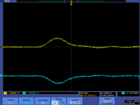
| |
| 3900 | 3600 | 870 | 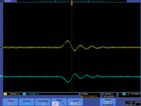
| |
| 3850 | 3550 | 859 | 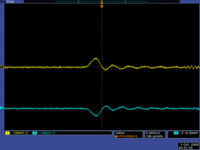
|
| TGEM Drift HV (Volts) | TGEM Drift current A | TGEM foil HV (Volts) | TGEM foil current A |
| 3600 | 3300 |
SIS310
1.) Get 100 Ohm resistors
2.) Get Bread board
10/3/08
The high current draw (> 1mA) of the TGEM on the power supply has forced us to switch to powering each PCboard GEM individually. We now have 4 HV channels hooked up with the ground floating on the top 2 GEM PCboards.
GEM Detector
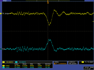
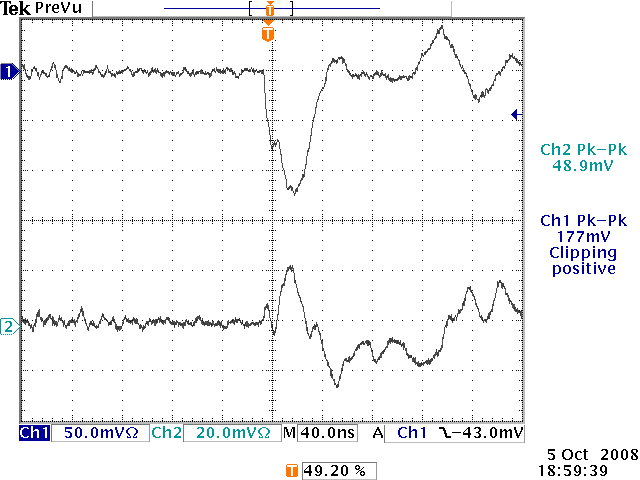
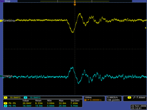
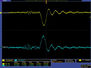
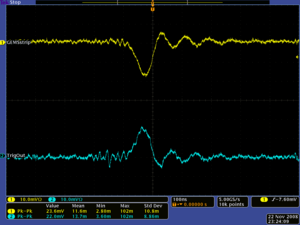
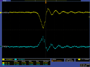
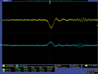
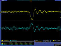
Vdrift = 3800, VGem = 3500, IDrift = 0, IGem = 842 A. Channel 1 is the output of 16 strips tied together. The remaining output strips have a 1 M Ohm resister to ground. Channel 2 is the Trigger output (the output from the last foil). Notice the sign difference between the 2 outputs.
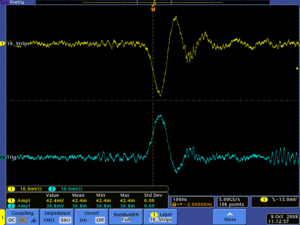
Vdrift = 3850, VGem = 3550, IDrift = 0, IGem = 858 A
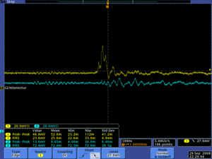
Output from the GEM detector strips and from TrigOut after signal goes through the Timing Filter Amp(amplifier was set to "x10").
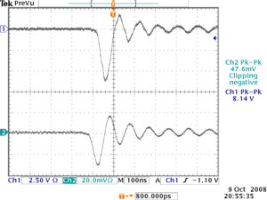
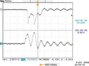
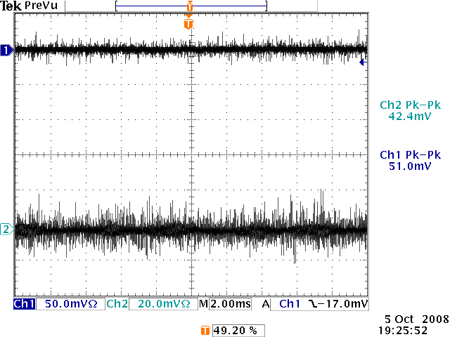
The output from GEM detector strips and TrigOut(after it goes through electronics):
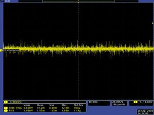
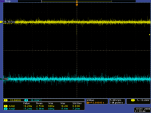
Noise level will be documented.
The GEM detector is working!
GEM DETECTOR IS READY WITH ELECTRONICS
THGEM Detector
Lets check the TGEM detector
Media:TheTHGEM_MasterThesis_Chen_Ken_Shalem.pdf
The distance between the THGEM foils is 2 mm(before it was ~1.5 mm) and the distance between the last THGEM foil and cathode is about ~5 mm. I have not changed the distance between the PCB(Charge collector) and the first THGEM foil.(might do it)
THGEM detector is not working still at high voltages.
For now HVSettings are following(I still have sparks, but they are very few, and I think they come from THGEM foils)
HVsettings
| Cathode HV (Volts) | First THGEM foil(Volts) | Second THGEM foil(Volts) | Third THGEM foil(Volts) | Third THGEM foil current A |
| 3000 | 1650 | 1500 | 1500 | 1181 |
11/21/08
a.)ship out Qweak GEM
Rectangular GEM detector works after replacing all 3 GEM preamp foils!!!!!!!!
Need to replace foils one at a time to see which one is bad and then determine why it is bad. Short?
Distance between the GEM foils are 2 mm. Distance between the last GEM foil and PCB is also 2 mm. The first GEM foil and cathode are separated by 3 mm.
Ramp Up = 2 Volts/sec.
Can go up to Volts without even one spark and Volts.
11-25-08
1.) One GEM foil is bad.
2.) Second GEM foil works:
High Voltage on Drift was 3800Volts and on GEM 3500 Volts.
3.) Third GEM foil works:
High Voltage on Drift was 3800Volts and on GEM 3500 Volts(Sparks).
I see spots on the above "working" GEM foils.  Let's leave them out and keep the three new ones in.

DONE
Why is the "1" GEM foil not working?
Do not know yet.
Testing DC
HV Settings:
| HV settings | ||
| Wire | Volts | |
| Sense | 1700 | |
| Field | -850 | |
| Guard | 850 | |
Gas type: ArCO2 (90/10).
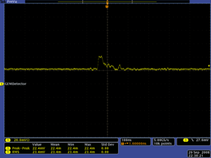
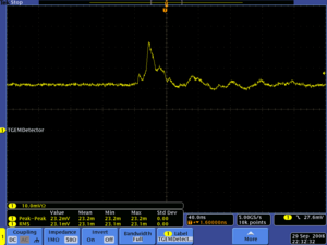
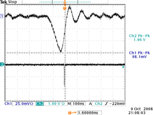
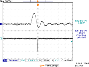
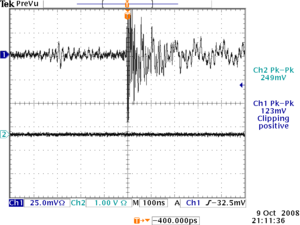
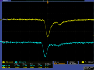
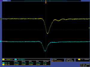
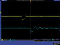
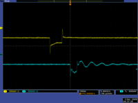
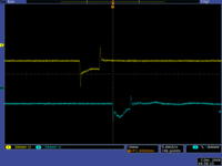
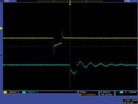
Below are shown the scope images of the signal from the DC(direct output from the sense wires):
Metalica
Plastika
Need UVA 122B Signal Splitter
PreAmp should be set to 6.5 Volts, otherwise we get the ring(noise level is high).
PreAmp, Chamber Amp && VPIPostAmp
What does the TDC output look like from the PostAmp. Does it drive our CAEN TDC?
Gas type: ArCO2 (90/10).
The voltage on PreAmp is set to 6.5 Volts.
HV Settings:
| HV settings | ||
| Wire | Volts | |
| Sense | 1500 | |
| Field | -750 | |
| Guard | 750 | |
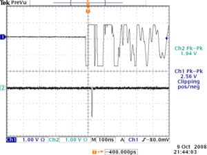
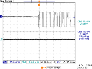
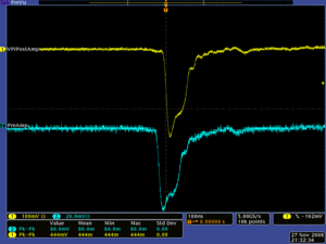
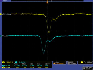
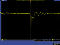
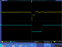
The signal outputs from the PreAmp and ChamberAmp compared for Metalica && Plastika.
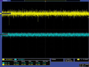
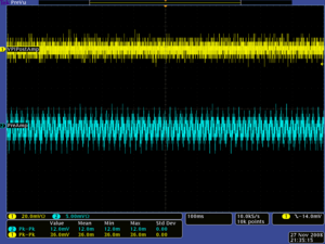
The signal outputs and noise level from the PreAmp and VPIPostAmp(TDC output) compared for Metalica && Plastika.
GEM 29-11-08
The strip output signal is used as a trigger and as a pulse too.
Gas type ArCO2 (90/10).
HV Settings: Volts and Volts.
Data: r564 and r571.
CAEN V775 TDC
From the results shown below one can make conclusions that the time interval between the end of the pulses effects the data.
The table below shows the TDC measurement made using the Stanford pulse generator to generate 2 ECL input pulses. The first pulse is defined to rise at point "A" in time and fall at point "B" in time. The second pulse rises at point "C" in time and falls at point "B" in time. Comparing the time intervals between the pulses to the TDC output indicates that the TDC measures the time interval BD.
| A | B | C | D | TDC | AC | AD | BC | BD |
| 0 | 60 | 150 | 200 | 2526 | 150 | 200 | 90 | 140 |
| 0 | 90 | 150 | 200 | 1942 | 150 | 200 | 60 | 110 |
| 0 | 90 | 150 | 230 | 2504 | 150 | 230 | 60 | 140 |
| 30 | 60 | 150 | 200 | 1927 | 120 | 170 | 90 | 140 |
| 30 | 60 | 130 | 200 | 2501 | 100 | 170 | 70 | 140 |
First case
A=T+0
B=A+60ns
C=T+150ns
D=T+200ns
-> c775Reset
value = 0 = 0x0
-> c775Status(0)
STATUS for TDC id 0 at base address 0x90610000
----------------------------------------------
Interrupts Disabled
Last Interrupt Count    : 0
            --1--  --2--
 S-> c775Reset
value = 0 = 0x0
-> c775Status(0)
STATUS for TDC id 0 at base address 0x90610000
----------------------------------------------
 Interrupts Disabled
 Last Interrupt Count    : 0
            --1--  --2--
  Status  = 0x0053 0x0000  (Data Ready)
  BitSet  = 0x0000 0x4880
  Control = 0x0000
  FSR     = 440 nsec
  Event Count     = 1
  Last Event Read = (No Events Read)
 value = 37 = 0x25 = '%'
-> c775PrintEvent
 TDC DATA for Module 0
 Header: 0xfa000100   nWords = 1
     0xf80249de
 Trailer: 0xfc000000   Event Count = 0
value = 3 = 0x3
->
TDC bits 100111011110 b = 2526 d
Second case
A=T+0
B=A+90ns
C=T+150ns
D=T+200ns
-> c775PrintEvent
 TDC DATA for Module 0
 Header: 0xfa000100   nWords = 1
     0xf8024796
 Trailer: 0xfc000003   Event Count = 3
value = 3 = 0x3
-> c775Status(0)
STATUS for TDC id 0 at base address 0x90610000
----------------------------------------------
Interrupts Disabled
Last Interrupt Count    : 0
            --1--  --2--
 Status  = 0x005f 0x0004  (Buffer Full)
 BitSet  = 0x0000 0x4880
 Control = 0x0000
 FSR     = 440 nsec
 Event Count     = 217
 Last Event Read = 3
value = 22 = 0x16
->
The TDC Bits 011110010110 b = 1942 d
Third case
A=T+0
B=A+90ns
C=T+150ns
D=T+230ns
-> c775Status(0)
STATUS for TDC id 0 at base address 0x90610000
----------------------------------------------
Interrupts Disabled
Last Interrupt Count    : 0
            --1--  --2--
 Status  = 0x0053 0x0000  (Data Ready)
 BitSet  = 0x0000 0x4880
 Control = 0x0000
 FSR     = 440 nsec
 Event Count     = 5
 Last Event Read = (No Events Read)
value = 37 = 0x25 = '%'
-> c775PrintEvent
 TDC DATA for Module 0
 Header: 0xfa000100   nWords = 1
     0xf80249c8
 Trailer: 0xfc000000   Event Count = 0
value = 3 = 0x3
->
TDC bits 100111001000 b = 2504 d
Fourth case
A=T+30ns
B=A+60ns
C=T+150ns
D=T+200ns
-> c775Status(0)
STATUS for TDC id 0 at base address 0x90610000
----------------------------------------------
Interrupts Disabled
Last Interrupt Count    : 0
            --1--  --2--
 Status  = 0x0053 0x0000  (Data Ready)
 BitSet  = 0x0000 0x4880
 Control = 0x0000
 FSR     = 440 nsec
 Event Count     = 5
 Last Event Read = (No Events Read)
value = 37 = 0x25 = '%'
-> c775PrintEvent
 TDC DATA for Module 0
 Header: 0xfa000100   nWords = 1
     0xf8014787
 Trailer: 0xfc000003   Event Count = 3
value = 3 = 0x3
->
TDC : 011110000111 b = 1927 d
Fifth case
A=T+30ns
B=A+60ns
C=T+130ns
D=T+200ns
-> c775Status(0)
STATUS for TDC id 0 at base address 0x90610000
----------------------------------------------
Interrupts Disabled
Last Interrupt Count    : 0
            --1--  --2--
 Status  = 0x0053 0x0000  (Data Ready)
 BitSet  = 0x0000 0x4880
 Control = 0x0000
 FSR     = 440 nsec
 Event Count     = 3
 Last Event Read = 0
value = 22 = 0x16
-> c775PrintEvent
 TDC DATA for Module 0
 Header: 0xfa000100   nWords = 1
     0xf80149c5
 Trailer: 0xfc000000   Event Count = 0
value = 3 = 0x3
->
TDC bits 100111000101 b = 2501 d
TDC AND DC
-> c775PrintEvent
 TDC DATA for Module 0
 Header: 0xfa000200   nWords = 2
     0xf80040e8  0xf80f415f
  Trailer: 0xfc000004   Event Count = 4
value = 4 = 0x4
Checking PMT
-> c775PrintEvent
 TDC DATA for Module 0
 Header: 0xfa001000   nWords = 16
     0xf8004252  0xf80140e9  0xf80240d3  0xf80340e5  0xf80440e5
     0xf80540f4  0xf80640ef  0xf807418a  0xf8084195  0xf80942d9
     0xf80a418b  0xf80b4184  0xf80c4140  0xf80d413d  0xf80e4152
     0xf80f414d
 Trailer: 0xfc000000   Event Count = 0
value = 18 = 0x12
-> c775PrintEvent
 TDC DATA for Module 0
 Header: 0xfa001000   nWords = 16
     0xf8004214  0xf8014172  0xf802415a  0xf80340af  0xf804416e
     0xf805417a  0xf806424a  0xf80740b5  0xf80841a5  0xf809419a
     0xf80a40b9  0xf80b4195  0xf80c418e  0xf80d40b2  0xf80e4193
     0xf80f4184
 Trailer: 0xfc000001   Event Count = 1
value = 18 = 0x12
