Difference between revisions of "TF EIM Chapt6"
| Line 7: | Line 7: | ||
*higher input impedance than bi-polar | *higher input impedance than bi-polar | ||
*less gain than bi-polar | *less gain than bi-polar | ||
| − | + | *better temperature stability | |
=JFET = | =JFET = | ||
Revision as of 03:08, 6 April 2011
Field Effect Transistors (FET, JFET, MOSFET)
Properties
FETs differ from the bipolar transistors in the las chapter in that the current from a FET is only due to the majority charge carriers in the semiconductor while bi-polar transistors current is produced from both carrier types; electron and hole.
- higher input impedance than bi-polar
- less gain than bi-polar
- better temperature stability
JFET
JFET Junction Field Effect Transistor
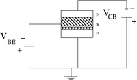
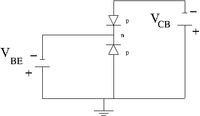
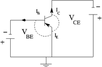
In a bi-polar transistor you have a depletion region with mixed charge carriers
 |
 |
|
| pnp bi-polar transistor | Equivalence circuit | Circuit diagram |
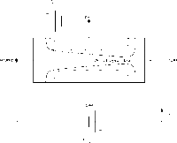
In the Junction Field Effect Transistor you have a single charge carrier with the minority charge carriers forming a choke point for the majority carrier current flow. It is similar to "pinching" a garden hose when water is flowing through it.
 |
 |
|
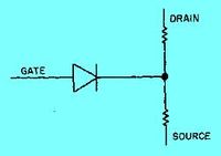
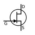
| JFET | Equivalence circuit | Circuit diagram |
The semiconductor material of the gate is the opposite of the channel. Here the n-p (or p-n) junction is between the gate and the channel.
The JFET operates by reverse biasing the gate-channel junction (diode) so the gate current doesn't flow in the direction indicated by the circuit diagram symbol. This means that the current through the gate is small (nAmps). As a result the input impedance looking into the gate is high (M) for the equivalent circuit.
The current junction rule is
for the Bi-Polar transistor
Resistance
The FET acts like a resistor.
Consider the following circuit
Let
the drain driving voltage
= resistor between the drain and V_{DD}
if = resistivity of the n-type semiconductor
then
- r = = resistance of the JFET
If you reverse bias the gate then the depletion region at the p-n junction expands into the n-type material thereby reducing the cross-sectional area (A) of the channel.
FET pinchoff
If you continue to reverse bias the gate, keeping V_{DD} constant, then the drain current will decrease as you make the gate more negative.
The pinchoff condition will occur when the reverse bias is large enough to stop the drain current I_D.
where
- = dielectric constant
- = thickness of the channel
- = number of impurity atoms per volume
Maximum drain current (current flows from Drain to Source with the gate Shorted; ie = 0)
MOSFET
MOSFET Metal-Oxide-Semiconductor Field Effect Transistor