Difference between revisions of "TF EIM Chapt4"
| (4 intermediate revisions by the same user not shown) | |||
| Line 34: | Line 34: | ||
:When you add the atoms to form the lattice, the potential barrier is lowered. This allows the electrons in the higher (more valence) states to become shared among adjacent atoms.( Delocalized) | :When you add the atoms to form the lattice, the potential barrier is lowered. This allows the electrons in the higher (more valence) states to become shared among adjacent atoms.( Delocalized) | ||
:Another effect is that the energy bands become wider. As the electrons in the higher energy states are shared between atoms forming a bond, the time any one electron spends bound to any one atom becomes smaller. SInce<math> \Delta E \Delta t \approx \hbar</math> one finds that <math>\Delta E</math> gets bigger for the higher state electrons (less bound) since their time \Delta t in a given bound state becomes less. The electron energy states become band like structures which get wider as you move to higher energy (less bound) electron states. | :Another effect is that the energy bands become wider. As the electrons in the higher energy states are shared between atoms forming a bond, the time any one electron spends bound to any one atom becomes smaller. SInce<math> \Delta E \Delta t \approx \hbar</math> one finds that <math>\Delta E</math> gets bigger for the higher state electrons (less bound) since their time \Delta t in a given bound state becomes less. The electron energy states become band like structures which get wider as you move to higher energy (less bound) electron states. | ||
| + | |||
| + | |||
| + | ;also | ||
| + | :The amount of energy needed for an electron to move from the valence region to the conduction region is known as <math>E_{gap}</math>. This gap energy is on the order of an election Volt (eV). The available thermal energy (kT) at room temperature is about 0.025 eV (1/40). At room temperature you would not expect to see an electron move from the valence region (band) to the conduction region (band). A battery though could be used to accomplish this by pulling valence electrons out of their bound states and putting them into the conduction region. Or you could heat up the material to 50 times room temperature. | ||
| Line 114: | Line 118: | ||
:<math>\rho(E) = \frac{2^{7/2}m^{3/2} \pi}{h^3}E^{1/2}=</math> density of states for electrons in a periodic crystal lattice | :<math>\rho(E) = \frac{2^{7/2}m^{3/2} \pi}{h^3}E^{1/2}=</math> density of states for electrons in a periodic crystal lattice | ||
| − | ::<math>= \frac{2^{7/2}m^{3/2} \pi}{h^3}(E-E_{gap})^{1/2}</math> | + | ::<math>= \frac{2^{7/2}m^{3/2} \pi}{h^3}(E-E_{gap})^{1/2}</math> = density of states for electrons in the conduction band where E=0 at the valence band |
| Line 131: | Line 135: | ||
:<math>N_{cb} = \int_{E_{gap}}^{\infty}N(E) dE = \int_{E_{gap}}^{\infty} \frac{2^{7/2}m^{3/2} \pi}{h^3}(E-E_{gap})^{1/2} \times e^{-\left( E-E_f\right)/kT}dE</math> | :<math>N_{cb} = \int_{E_{gap}}^{\infty}N(E) dE = \int_{E_{gap}}^{\infty} \frac{2^{7/2}m^{3/2} \pi}{h^3}(E-E_{gap})^{1/2} \times e^{-\left( E-E_f\right)/kT}dE</math> | ||
| − | ::<math>= \frac{2^{5/2}(m\pi kT)^{3/2} }{h^3}e^{-E_{gap}/2kT}</math> | + | ::<math>= \frac{2^{5/2}(m\pi kT)^{3/2} }{h^3}e^{-E_{gap}/2kT}</math> : <math>E_F= E_{gap}/2</math> |
:: <math>= 4.6 \times 10^{15} \frac{\mbox{electrons}}{\mbox{cm}^3 \mbox{degree K}^{3/2}} T^{3/2}e^{-E_{gap}/2kT}</math> | :: <math>= 4.6 \times 10^{15} \frac{\mbox{electrons}}{\mbox{cm}^3 \mbox{degree K}^{3/2}} T^{3/2}e^{-E_{gap}/2kT}</math> | ||
:: <math>\propto T^{3/2}e^{-E_{gap}/2kT}</math> | :: <math>\propto T^{3/2}e^{-E_{gap}/2kT}</math> | ||
| Line 167: | Line 171: | ||
| − | [[File:TF_EIM_SiliconLattice_np_junction.jpg| | + | [[File:TF_EIM_SiliconLattice_np_junction.jpg| 400 px]][[File:TF_EIM_p-n_junction.jpg| 400 px]] |
Note: The material still has a net charge of zero. The semi-conductor has excess FREE electrons on the n-side and excess HOLES on the p-side of the junction. Notice this looks like a charged up capacitor with a voltage difference to be in order for charge to move/conduct. | Note: The material still has a net charge of zero. The semi-conductor has excess FREE electrons on the n-side and excess HOLES on the p-side of the junction. Notice this looks like a charged up capacitor with a voltage difference to be in order for charge to move/conduct. | ||
| Line 177: | Line 181: | ||
The "depletion" region is located at the junction and is a place which has been "depleted" of mobile charge carriers. The ionized acceptor and donor impurity atoms are fixed in the crystal lattice at the junction. | The "depletion" region is located at the junction and is a place which has been "depleted" of mobile charge carriers. The ionized acceptor and donor impurity atoms are fixed in the crystal lattice at the junction. | ||
| − | [[File:TF_EIM_PotBarrier_p-n_junct.jpg | | + | [[File:TF_EIM_PotBarrier_p-n_junct.jpg | 400 px]] |
Revision as of 18:29, 19 February 2015
Semiconductor physics
There are 5 states of matter: Solid, liquid, gas, plasma (ionized gas) , and a Bose-Einstein condensate (quantum effects on a macroscopic scale).
Crystal Lattice
Semiconductor physics focuses on the solid state of matter in the form of crystals.
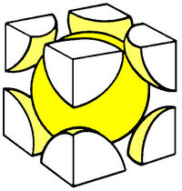
Crystals are formed when atoms are arranged in repeating structures called the crystal lattice. The recurrent structure which forms the crystal lattice is referred to a a cell.
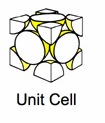
Some popular cell names are
 |
 |
|
| (SC) Simple Cubic | (BCC) Body Centered Cubic | (FCC) Face Centered Cubic |
The above images are suppose to represent the distribution of electrons in the crystal lattice cell.
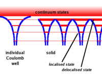
To understand this structure more let's consider the structure of a 1-D crystal of atoms
A single free atom will have electrons bound to the atom due to the coulomb force. The bound electrons are found in various energy levels.
- Notice
- When you add the atoms to form the lattice, the potential barrier is lowered. This allows the electrons in the higher (more valence) states to become shared among adjacent atoms.( Delocalized)
- Another effect is that the energy bands become wider. As the electrons in the higher energy states are shared between atoms forming a bond, the time any one electron spends bound to any one atom becomes smaller. SInce one finds that gets bigger for the higher state electrons (less bound) since their time \Delta t in a given bound state becomes less. The electron energy states become band like structures which get wider as you move to higher energy (less bound) electron states.
- also
- The amount of energy needed for an electron to move from the valence region to the conduction region is known as . This gap energy is on the order of an election Volt (eV). The available thermal energy (kT) at room temperature is about 0.025 eV (1/40). At room temperature you would not expect to see an electron move from the valence region (band) to the conduction region (band). A battery though could be used to accomplish this by pulling valence electrons out of their bound states and putting them into the conduction region. Or you could heat up the material to 50 times room temperature.
There are 14 different Bravais lattice configurations
| Crystal System | Lattice type |
| Cubic | Simple, Face Centered, Body Centered |
| Tetragonal | Simple, Body Centered |
| Orthorhombic | Simple, Face Centered, Body Centered, End Centered |
| Monoclinic | Simple, End Centered |
| Rhombohedral | Simple |
| Triclinic | Simple |
| Hexagonal | Simple |
Most Semiconductors are made from Silicon and GaAs.
Silicon is a Face Centered Cubic cell
Silicon is an insulator if in pure form with 4 weakly bound (valence) electrons.
If you replace silicon atoms in the lattice with atoms that have either 3 valance or 5 valence electrons (doping) your can create sites with either a deficient number of electrons (a missing bond) or extra electrons (complete bond with a free electron)
By Doping silicon you can create sites with extra electrons (n-type) or sites with a deficient number of electrons (vacancies or holes ) (P-type)
Fermi-Dirac Statistics
As seen above, the properties of a semi-conductor will be determined by the electron configuration in the crystal lattice. In particular, the distribution of electrons in the conduction band of the lattice since those are the electrons which can move in the crystal in response to an applied electric field (voltage) as produce observable effect.
Pauli Exclusion Principle
The Pauli exclusion principle states that no two electrons may occupy the same quantum state. This principle is seen by the quantum energy levels of electrons bound to atoms.
An important consequence of this principle is that, an crystal composed of atoms will filled energy bands is an insulator. You can only conduct electrons if there is an energy state available for the electron to populate. An electric field is established by applying a potential difference which pushes an electron up to a partially filled available energy state that is shared between the atoms in the lattice, thereby allowing the electron to "travel" to adjacent atoms.
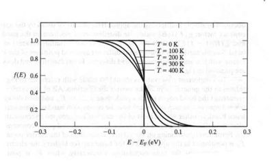
Fermi Function (F[E])
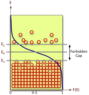
The energy levels in a crystal lattice may be grouped into a conduction band and a valence band that are separated by a forbidden energy region called the band gap.
the probability that a given energy level is occupied by an electron.
using Statistical Thermodynamic one can calculate the above Fermi function as
where
- Fermi energy of the given crystal lattice
- temperature of lattice in Kelvin
- Note
- At room temperature: kT = 1/40 eV
- (half of the energy needed to move from the valence to the conduction band
Electron Energy Distribution
The number of electrons per unit volume within the energy band is represented as
where
- density of states for electrons in a periodic crystal lattice
- = density of states for electrons in the conduction band where E=0 at the valence band
When is in the conduction band
or
The total number of electrons in the conduction band is
-
- :
Where
- Note: usually makes the exponential term more dominant than the term.
For the two common semi-conductors of Germainum and Silicon at room temperature we have
How much current can this be?
if we assume
cross-sectional area of the wire = electron drift velocity for Germanium when an electric field of 10V/cm is applied through the wire.
Then
A detectable current but not high enough for practical applications
The P-N junction Diode/rectifier
Returning back to the picture of a silicon lattice doped with Boron (3 instead of 4 valence e-; hole; acceptor atom) and Phosphorus ( 5 instead of 4 valence electrons; electron, donor atom).
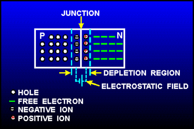
Note: The material still has a net charge of zero. The semi-conductor has excess FREE electrons on the n-side and excess HOLES on the p-side of the junction. Notice this looks like a charged up capacitor with a voltage difference to be in order for charge to move/conduct.
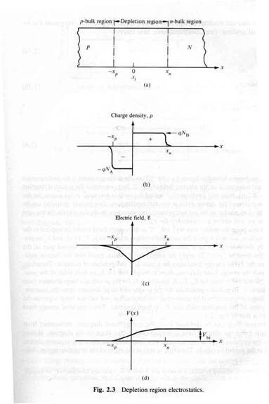
AN electric field in the depletion region points from the n-type (donor) side to the p-type (acceptor) side. Electrons near the junction are pulled toward the n-type material and holes are pulled to the p-type material.
This electric field results in an effective voltage , where is the thickness of the depletion region.
The "depletion" region is located at the junction and is a place which has been "depleted" of mobile charge carriers. The ionized acceptor and donor impurity atoms are fixed in the crystal lattice at the junction.
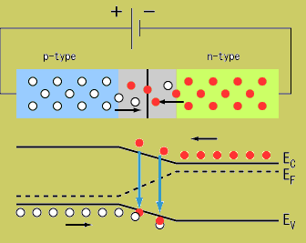
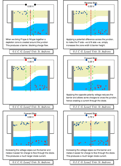
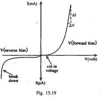
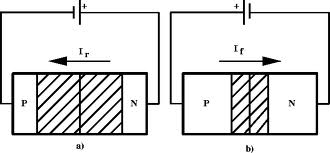
A forward biasing of the above p-n junction means that you oppose the direction of the junction field. The positive side of the battery is put on the "p" side of the junction and the negative side on the "n" side of the junction. This reduces the junction barrier (squeezes the depletion region) making it easier for current to flow through the junction. The bias electric field is directed opposite to the depletion electric field . When you reverse bias the p-n junction you are increasing the junction barrier making it harder for current to flow. At some point though, the junction will break down and you will force current to flow.
|
| Notice the depletion region expands for the reverse biased example on the left. The depletion region narrows when the p-n junction is in the forward biased orientation. |
If you try and push current in the opposite direction you have an even higher barrier (step potential) to overcome than in the forward direction. There are only "holes" on the p-type side of the junction so electrons need to be "freed" by breaking covalent bonds on the p-type material side thereby creating 2 new charge carriers, one for the hole and one free to move to the n-type side. The bond breaking potential is higher than the potential needed to overcome the difference in Fermi energies.
Voltage Rectification
Electrical power is usually supplied as a high voltage AC source.
- Do you remember the reason AC is used to distribute electricity?
- Most power is generator via a mechanical means where a loop of wire (coil) is rotated in a magnetic field.
- Less power is lost through a traveling AC current than a DC current. , is a constant property of the transmission line
Laptops and other electronic devices usually use DC.
- How does the AC-to-DC adapter work?
Half Wave rectifier
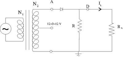
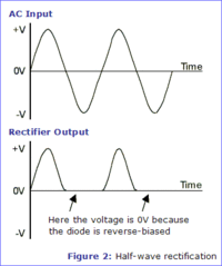
A half wave rectifier is a circuit which passes only half of the input AC waveform.
This is accomplished by using the diode's forward drop voltage to "clip" the AC signal.
Consider the following circuit
The Transformer
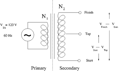
A transformer uses inductors/coils to step voltages either up or down based on the ratio of the number of coil turns and .
Let represent the magnetic flux seen by the inductors due to the changing current in the primary.
- = Input Voltage on the Primary side
- = Output Voltage on the Secondary
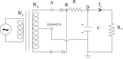
The ground is relative for a transfer. You could use the "Tap" or center post as a ground and either the Start or Finish end
- = Output voltage between Tap and Secondary
Where ground
Since both coils see the same flux
If you have a step UP (Voltage increasing) Transformer
If you have a step DOWN (Voltage decreasing) Transformer
The Clipping Circuit
The negative voltage is clipped as long as the input voltage does not exceed the reverse breakdown voltage.
Diodes have rating for both the break down voltage and the max current that can be passed in the forward direction.
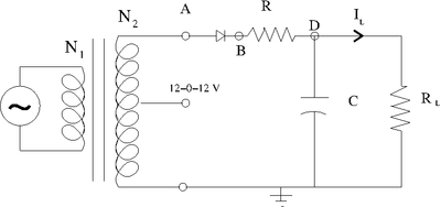
Constant DC with Ripple
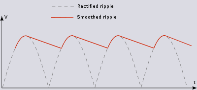
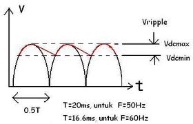
This circuit adds an RC low-pass filter so the voltage will slowly drop, according to the RC time constant, while the AC current is on its opposite swing.
The ripple's voltage drop is determined by the capacitor selected.
- Larger current becomes larger ripple. The larger the capacitor the smaller the ripple!
For a given current, select the voltage change you want for the ripple (\Delta V} and use the time between the peaks of the output (\Delta t) to detemine the Capacitor you need for the desired ripple.
Ex: Assume a 60 Hz AC current of I = 1mA and ask that V ; sec
- Caution
- Be sure the Resistors can support the power!
Full wave
The Full wave is more efficient than the half wave because it does not block half of the current but inverts it.
The desired ripple is again given by
But this time time \Delta t is half as long (1/120 sec) because you didn;t through away half of the current
Ex: Assume a 60 Hz AC current of I = 1mA and ask that V ; sec
Applications
Amplitude Modulation (AM Radio)
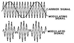
The Amplitude Modulated Voltage (V_{AM}) will be a function of the Carrier wave voltage (V_C) such that
where
- = amount of modulation
- modulation frequency
