Difference between revisions of "TF EIM Chapt3"
| Line 134: | Line 134: | ||
:<math>N_{cb} = \int_{E_{gap}}^{\infty}N(E) dE = \int_{E_{gap}}^{\infty} \frac{2^{7/2}m^{3/2} \pi}{h^3}(E-E_{gap}^{1/2} \times e^{-\left( E-E_f\right)/kT}dE</math> | :<math>N_{cb} = \int_{E_{gap}}^{\infty}N(E) dE = \int_{E_{gap}}^{\infty} \frac{2^{7/2}m^{3/2} \pi}{h^3}(E-E_{gap}^{1/2} \times e^{-\left( E-E_f\right)/kT}dE</math> | ||
::<math>= frac{2^{5/2}(m\pi kT)^{3/2} }{h^3}e^{-E_{gap}/2kT}</math> | ::<math>= frac{2^{5/2}(m\pi kT)^{3/2} }{h^3}e^{-E_{gap}/2kT}</math> | ||
| + | :: <math>= 4.6 \times 10^{15} \frac{\mbox{electrons}}{\mbox{cm}^3 \mbox{degree K}^{-3/2}} T^{3/2}e^{-E_{gap}/2kT}</math> | ||
| + | :: <math>\propto T^{3/2}</math> | ||
Where | Where | ||
Revision as of 06:13, 15 February 2011
Semiconductor physics
There are 5 states of matter: Solid, liquid, gas, plasma (ionized gas) , and a Bose-Einstein condensate (quantum effects on a macroscopic scale).
Crystal Lattice
Semiconductor physics focuses on the solid state of matter in the form of crystals.
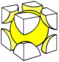
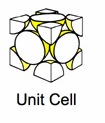
Crystals are formed when atoms are arranged in repeating structures called the crystal lattice. The recurrent structure which forms the crystal lattice is referred to a a cell.
Some popular cell names are
 |
 |
|
| (SC) Simple Cubic | (BCC) Body Centered Cubic | (FCC) Face Centered Cubic |
The above images are suppose to represent the distribution of electrons in the crystal lattice cell.
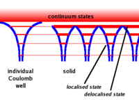
To understand this structure more let's consider the structure of a 1-D crystal of atoms
A single free atom will have electrons bound to the atom due to the coulomb force. The bound electrons are found in various energy levels.
- Notice
- When you add the atoms to form the lattice, the potential barrier is lowered. This allows the electrons in the higher (more valence) states to become shared among adjacent atoms.( Delocalized)
- Another effect is that the energy bands become wider. As the electrons in the higher energy states are shared between atoms forming a bond, the time any one electron spends bound to any one atom becomes smaller. SInce one finds that gets bigger for the higher state electrons (less bound) since their time \Delta t in a given bound state becomes less. The electron energy states become band like structures which get wider as you move to higher energy (less bound) electron states.
There are 14 different Bravais lattice configurations
| Crystal System | Lattice type |
| Cubic | Simple, Face Centered, Body Centered |
| Tetragonal | Simple, Body Centered |
| Orthorhombic | Simple, Face Centered, Body Centered, End Centered |
| Monoclinic | Simple, End Centered |
| Rhombohedral | Simple |
| Triclinic | Simple |
| Hexagonal | Simple |
Most Semiconductors are made from Silicon and GaAs.
Silicon is a Face Centered Cubic cell
Silicon is an insulator if in pure form with 4 weakly bound (valence) electrons.
If you replace silicon atoms in the lattice with atoms that have either 3 valance or 5 valence electrons (doping) your can create sites with either a deficient number of electrons (a missing bond) or extra electrons (complete bond with a free electron)
By Doping silicon you can create sites with extra electrons (n-type) or sites with a deficient number of electrons (vacancies or holes ) (P-type)
Fermi-Dirac Statistics
As seen above, the properties of a semi-conductor will be determined by the electron configuration in the crystal lattice. In particular, the distribution of electrons in the conduction band of the lattice since those are the electrons which can move in the crystal in response to an applied electric field (voltage) as produce observable effect.
Pauli Exclusion Principle
The Pauli exclusion principle states that no two electrons may occupy the same quantum state. This principle is seen by the quantum energy levels of electrons bound to atoms.
An important consequence of this principle is that, an crystal composed of atoms will filled energy bands is an insulator. You can only conduct electrons if there is an energy state available for the electron to populate. An electric field is established by applying a potential difference which pushes an electron up to a partially filled available energy state that is shared between the atoms in the lattice, thereby allowing the electron to "travel" to adjacent atoms.
Fermi Function (F[E])
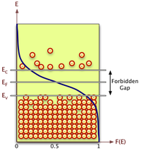
The energy levels in a crystal lattice may be grouped into a conduction band and a valence band that are separated by a forbidden energy region called the band gap.
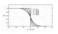
the probability that a given energy level is occupied by an electron.
using Statistical Thermodynamic one can calculate the above Fermi function as
where
- Fermi energy of the given crystal lattice
- temperature of lattice in Kelvin
- Note
- At room temperature: kT = 1/40 eV
- (half of the energy needed to move from the valence to the conduction band
Electron Energy Distribution
The number of electrons per unit volume within the energy band is represented as
where
- density of states
When is in the conduction band
or
The total number of electrons in the conduction band N_{cb} is
Where
