Difference between revisions of "Readout Electronics"
(→Timing) |
|||
| (One intermediate revision by the same user not shown) | |||
| Line 28: | Line 28: | ||
:Progammable through the Latency register (8 bits = 256 bits) you have but only 128 registers data registers. We can go back in time 100 *32 ns = 3 micro seconds. But we only may need 100 ns. | :Progammable through the Latency register (8 bits = 256 bits) you have but only 128 registers data registers. We can go back in time 100 *32 ns = 3 micro seconds. But we only may need 100 ns. | ||
: | : | ||
| + | |||
| + | |||
| + | The cables lengths from the detector to the patch panel in dog house are | ||
| + | 150ns for both GEM A and GEM B. So the full lengths to the patch panel at | ||
| + | the second floor are 505+150 = 655ns for GEM A and 510+150 = 660ns | ||
| + | for GEM B. | ||
| + | |||
==V1495: can have programmable delay up to?== | ==V1495: can have programmable delay up to?== | ||
| Line 140: | Line 147: | ||
You need to power cycle or reset the module for the new firmware to be used. | You need to power cycle or reset the module for the new firmware to be used. | ||
| + | |||
| + | == compiling new library == | ||
| + | |||
| + | source ~/CODA/2.5/coda.setup | ||
| + | |||
| + | /home/daq/CODA/2.5/x86-linux/bin/ccppc -fno-builtin -fno-for-scope -fstrength-reduce -mlongcall -mcpu=604 -DCPU=PPC604 -DVXWORKS -D_GNU_TOOL -DVXWORKSPPC -I/usr/local/coda/2.5/common/include/ -I../h -c -o v1495Lib.o v1495Lib.c | ||
=FPGA to VME data transfer= | =FPGA to VME data transfer= | ||
Latest revision as of 18:55, 4 August 2010
I/O
Inputs to breakout box
- Trigger (LVDS)
- Clock ( RF synced pulse 31 MHz = 499/16 MHz, LVDS)
- Flip Flop scaner (1 TTL pulse)
V1495 :
- 28 Pin output on 34 pin ribbon cables
- Inputs to V1495:
- 180 bits of data = 12 bits Bunch Counter ( =31 MHz clock) + 12 bit (Event Counter + flags) + 12 bits (Chip ID) + 128 bits (data) + 16 bits (Checksum)
- The input register has been set to a size of 256 bit and there are 12 of them
Timing
- VFAT:
- Progammable through the Latency register (8 bits = 256 bits) you have but only 128 registers data registers. We can go back in time 100 *32 ns = 3 micro seconds. But we only may need 100 ns.
The cables lengths from the detector to the patch panel in dog house are
150ns for both GEM A and GEM B. So the full lengths to the patch panel at
the second floor are 505+150 = 655ns for GEM A and 510+150 = 660ns
for GEM B.
V1495: can have programmable delay up to?
We can program delays and play with the timing by downloading values for "lat" into the VFAT extended register and set delay on the V1495 through the ROC.
The V1495 can also interupt the VME backplane telling a ROC to readout the planes.
V1495 Install at JLab
ssh cdaq@gw-qweak.jlab.org
telnet qweakvme2
ssh root@gemgumstix.jlab.org
ssh root@gemgumstix1.jlab.org
Set Address
The GW ROC appears to be A24 so I changed SW4 from a "8" to a "9".
| Address | |
| Pin | Setting |
| SW 3 | 0 |
| SW 4 | 9 |
| SW 7 | 3 |
| SW 8 | 3 |
Initialize module
No LEDs were on when the module is inserted into VME
-> v1495Init(0x09330000)
0x1a6c490 (tShell): v1495Init: v1495 Module has been successfully initialized.

0x1a6c490 (tShell): v1495 module has been reset:

value = 0 = 0x0
Check the modules is at adress
The base address offset in the Weiner ROC is 10 for A32 and 11 for A24
--> v1495test(0x11330000)
0x1a796e0 (tShell): Control      [0x11338000] = 0x0000
0x1a796e0 (tShell): firmwareRev  [0x1133800c] = 0x0001
0x1a796e0 (tShell): selflashVME  [0x1133800e] = 0x0001
0x1a796e0 (tShell): flashVME     [0x11338010] = 0x00ff
0x1a796e0 (tShell): selflashUSER [0x11338012] = 0x0001
0x1a796e0 (tShell): flashUSER    [0x11338014] = 0x00ff
0x1a796e0 (tShell): configROM    [0x11338100] = 0x00ec
value = 0 = 0x0
now download the firmware
Had to copy the *.rbf file to the directory in which the ROC is pointing to /coda/libraries/vme/v1495_gem
-> v1495firmware(0x11330000,"GEMReadout_Rev2-3_32Mhz.rbf",0,0)
0x1a796e0 (tShell):
0x1a796e0 (tShell): ********************************************************
0x1a796e0 (tShell): * CAEN SpA - Front-End Division                        *
0x1a796e0 (tShell): * ---------------------------------------------------- *
0x1a796e0 (tShell): * Firmware Upgrade of the V1495                        *
0x1a796e0 (tShell): * Version 1.1 (27/07/06)                               *
0x1a796e0 (tShell): *   Sergey Boyarinov: CLAS version 23-Apr-2007         *
0x1a796e0 (tShell): ********************************************************

0x1a796e0 (tShell): Updating firmware of the FPGA USER with the file GEMReadout_Rev2-3_32Mhz.rbf
0x1a796e0 (tShell): End of file: bp=113 bcnt=168545
0x1a796e0 (tShell):
Firmware loaded successfully. Written 168545 bytes
0x1a796e0 (tShell):
0x1a796e0 (tShell): Reloading user FPGA firmware...0x1a796e0 (tShell): done!
value = 0 = 0x0
The DSTACK light turned green and blinked during the download. After the firmware was download the USER led blinked red and yellow.
I decided to download the NoPPL file so we don't run with Phase Lock Loop
-> v1495firmware(0x11330000,"GEMReadout_Rev2-3_NoPLL.rbf",0,0)
Now the User light blinks green
Upgrade system Firmware
the output of v1495test showed that the V1495 is running version 0.1 firmware so I upgraded it to V 0.3 via the following
1.) Download the latest firmware from the CAEN web site
2.) The following command should download new firmware onto the module (notice the last number is a "1" instead of a "0" now)
-> v1495firmware(0x11330000,"V1495vme03.rbf",0,1)
There is a red switch on the module, if you screw this up, which can switch to a backup of the firmware.
You need to power cycle or reset the module for the new firmware to be used.
compiling new library
source ~/CODA/2.5/coda.setup
/home/daq/CODA/2.5/x86-linux/bin/ccppc -fno-builtin -fno-for-scope -fstrength-reduce -mlongcall -mcpu=604 -DCPU=PPC604 -DVXWORKS -D_GNU_TOOL -DVXWORKSPPC -I/usr/local/coda/2.5/common/include/ -I../h -c -o v1495Lib.o v1495Lib.c
FPGA to VME data transfer
On 2/15/07 Ben Raydo tested the read and write speeds between the VPM backplane and the FPGA user registers. He was able to write 16 bits to USER FPGA in 330 ns.
VFAT controls
Brian Oborn: 282- 6243
VFAT control registers
Control register 0
| bit | bit name | Function |
| 0 | Sleep/Run | 0 = sleep, 1=run also reffereed to as sleep blocking |
Control Register 1
Control register 2
VFAT Clock and Trig pulses
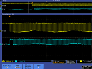
The Clock and Trigger LVDS pulses for the VFAT board were generated using the SIS3610 I/O register. I simply wrote bits to the register. The I/O registers internal clock then determine the pulse frequency. I set the bits to be 1110000000000000 using the command
s3610VFATclock(0,57344);
and reset all bits to zero except for the trigger input (100000000000000 b = 16384 d )which remained high for the first 3 clock pulses by hardwiring the value 16384 in the SIS3610 library function call. According to Table 2 in the VFAT manual from July 2006, leaving the first 3 bits high tells the VFAT board to operate in "CalPulse" mode..
 void s3610VFATclock(int id, unsigned int val)
 {

  int i;

  if((id<0) || (s3610p[id] == NULL)) {
    logMsg("s3610WriteOutput: ERROR : SIS3610 id %d not initialized \n",id,0,0,0,0,0);
    return;
  }

  s3610p[id]->d_out = val;
  s3610p[id]->d_out = 16384;
  s3610p[id]->d_out = val;
  s3610p[id]->d_out = 16384;
  s3610p[id]->d_out = val;
  s3610p[id]->d_out = 16384;

  for(i=0;i<200;i++)
    {
      s3610p[id]->d_out = val;
      s3610p[id]->d_out = 0;
    }

  logMsg("s3610VFATclock: Finish pulses \n",id,0,0,0,0,0);
  return;
}
The third highest bit was used to drive the scope.
To use the above function you need to be sure the SIS3610 is initialized by typing in the ROC communication window (telnet roc1)
-> s3610Init 0x3800
Initialized SIS3610 ID 0 at address 0x91003800
value = 0 = 0x0
The just execute the function
-> s3610VFATclock(0,57344);
0xdc79380 (tShell): s3610VFATclock: Finish pulses
value = 32 = 0x20 = ' '
Then using the Gumstick command line set the DFtest pattern bit via I2C
Turn on the VFAT
# pwd
/root/bin
# ./run.arm
set the DF test pattern bit
# echo "e 134 4 on" | flipbit.arm
Using mode e
Using address 134
Using bit 4
Using action on
Then in the ROC window exectue the VFAT clockpulse function
-> s3610VFATclock(0,57344);
0xdc79380 (tShell): s3610VFATclock: Finish pulses
value = 32 = 0x20 = ' '
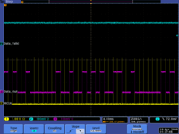
You should see the picture above
Put the VFAT back into sleep mode
# ./sleep_on.arm
Cal pulse Procedure
Check that VCAL connects to DACo
There is a new flipbit program now so the commands below will not work
1.) First set up the following values for operating the chip
| Register | Value |
| ContReg0 | 9 d = 1001 b |
| ContReg1 | 128 d = 10000000 b |
| IPreampIn | 142d = 10001110 b |
| IPreampFeed | 70 d = 1000110 b |
| IPreampOut | 130 d = 10000010 b |
| IShaper | 127 d = 1111111 b |
| IShaperFeed | 85 d = 1010101 b |
| IComp | 100 d = 1100100 b |
| vcal | 128 d = 10000000 b |
| Vthreshold1 | 0 |
| Vthreshold2 | 15 d = 1111 b |
1.) Connect VCal to DACo-V by setting DACsel = 1001
echo "p 65 0 on p 65 1 off p 65 2 off p 65 3 on" | flipbit.arm
2.) set calibration mode to output VCal values by setting CalMode = 01
echo "p 64 6 on p 64 7 off p " | flipbit.arm
3.) set VCAL
this turns one of the 8 bits to the calibration voltage Vcal (It ranges from 1.074 to 0.877 Volts)
echo "e 129 1 on" | flipbit.arm
4.) Look for a voltage on the output connector pin #162 which corresponds to pin B4 on the ribbon cable connector.
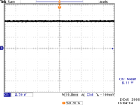
I see the following on the scope when I set VCAL to zero
echo "e 129 7 off" | flipbit.arm
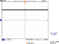
I see the following when I set the highest bit to VCAL (VCAL = 1000000 b = 128 d)
echo "e 129 7 on" | flipbit.arm
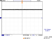
I see the following when I set the highest bit to VCAL (VCAL = 1111111 b = 255 d)
echo "e 129 7 on" | flipbit.arm
| VCAL | DC Level |
| 0 | 6.11 |
| 128 | 5.6 |
| 255 | 5.06 |
The VFAT2 manual states that VCAL should range between 1.074 to 0.877 Volts. I observe on the scope that the B4 pin output (VCAL) changes from 6.11 to 5.06 Volts when terminated in 1 M Ohm (High -Z).
I see the voltage difference between the min and max VCAL setting is 1.05 Volts. Perhaps this is what the manual refers to as the VCAL range?
VCAL baseline
The second step is to measure the baseline for each VCal DAC setting by changing calmode to (CalMode<1> =1 and clamod<0>=0). Above we had CalMode<1> =1 and CalMode<0>=1.
echo "p 64 6 off p 64 7 on p " | flipbit.arm
| VCAL | DC Level |
| 0 | 6.12 |
| 128 | 5.6 |
| 255 | 5.06 |
I see similar voltage on DAC-0 when I look at the baseline.
When I put the VFAT into sleep mode I see 26 mV on the output.
Setting Thresholds
The registers VThreshold1 and VThreshold2 are used to set the threshold on the analog input. The actual threshold applied is given by the difference (VTheshold2 -Vthreshold1) in order to have the ability to set positive and negative thresholds. A negative threshold (for the GEM output signal) can be set by having VThreshold2 =0 and VThreshold1>0.
Using VCAL to test output digitization
You can use VCal to inject a pulse into the channels via the CalChan1 bit on each channel. You need to be sure CalPolarity is consistent with (VTheshold2-VThreshold1).
I have a scipt to setup the VFAT parameters call cal.setup
from the gumstick console type the following within the /user/bin subdirectory:
# flipbit.arm < cal.setup
The web interface to the VFAT looked like
| ContReg<0> | 64 | 9 | 9 | ||||
| CalMode<1> | CalMode<0> | CalPolarity | MSPolarity | Trigmode<2> | Trigmode<1> | Trigmode<0> | Sleepb |
| Off | Off | Off | Off | On | Off | Off | On |
| ContReg<1> | 65 | 80 | 128 | ||||
| ReHitCT<1> | ReHitCT<0> | LVDSPowerSave | ProbeMode | DACsel<3> | DACsel<2> | DACsel<1> | DACsel<0> |
| On | Off | Off | Off | Off | Off | Off | Off |
| IPreampIn | 66 | 8e | 142 | ||||
| IPreampFeed | 67 | 46 | 70 | ||||
| IPreampOut | 68 | 82 | 130 | ||||
| IShaper | 69 | 7f | 127 | ||||
| IShaperFeed | 70 | 55 | 85 | ||||
| IComp | 71 | 64 | 100 | ||||
| ChipID<0> | 72 | f3 | 243 | ||||
| ChipID<1> | 73 | ee | 238 | ||||
| UpsetReg | 74 | 0 | 0 | ||||
| HitCount0 | 75 | 0 | 0 | ||||
| HitCount1 | 76 | 0 | 0 | ||||
| HitCount2 | 77 | 0 | 0 | ||||
| ExtRegPointer | 78 | 6 | 6 | ||||
| ExtRegData | 79 | 0 | 0 | ||||
| Lat | 0 | 0 | 0 | ||||
| VCal | 129 | 80 | 128 | ||||
| VThreshold1 | 130 | 0 | 0 | ||||
| VThreshold2 | 131 | f | 15 | ||||
| CalPhase | 132 | 0 | 0 | ||||
| ContReg<2> | 133 | 70 | 112 | ||||
| DigInSel | MSPulseLength<2> | MSPulseLength<1> | MSPulseLength<0> | HitCountSel<3> | HitCountSel<2> | HitCountSel<1> | HitCountSel<0> |
| Off | On | On | On | Off | Off | Off | Off |
| ContReg<3> | 134 | 5 | 5 | ||||
| - | - | - | DFTestPattern | PbBG | TrimDACrange<2> | TrimDACrange& lt;1> | TrimDACrange<0> |
| Off | Off | Off | Off | Off | On | Off | On |
| Spare<135> | 135 | ef | 239 | ||||
| ChanReg<1> | 1 | 10 | 16 | ||||
| CalChan0 | CalChan1 | Mask | TrimDAC<4> | TrimDAC<3> | TrimDAC<2 > | TrimDAC<1> | TrimDAC<0> |
| Off | Off | Off | On | Off | Off | Off | Off |
| ChanReg<2> | 2 | d0 | 208 | ||||
| CalChan1 | Mask | TrimDAC<4> | TrimDAC<3> | TrimDAC<2> | TrimDAC<1> | TrimDAC<0> | |
| On | On | Off | On | Off | Off | Off | Off |
| ChanReg<3> | 3 | 80 | 128 | ||||
| CalChan1 | Mask | TrimDAC<4> | TrimDAC<3> | TrimDAC<2> | TrimDAC<1> | TrimDAC<0> | |
| On | Off | Off | Off | Off | Off | Off | Off |
| ChanReg<4> | 4 | 0 | 0 | ||||
| CalChan1 | Mask | TrimDAC<4> | TrimDAC<3> | TrimDAC<2> | TrimDAC<1> | TrimDAC<0> | |
| Off | Off | Off | Off | Off | Off | Off | Off |
Now lets set CalMode to 01 so that the value of CalOut = VCAL
# echo "p 64 6 on" | flipbit.arm
# echo "p 64 7 off" | flipbit.arm
Now lets set the bit CalChan in channel 2 so the DAC output voltage is sent to Channel 2
# echo "e 2 6 on" | flipbit.arm
For channel 1 set TrimDAC= 1000 ( TrimDAC(4) =1 all others zero)
echo "e 1 1 off e 1 2 off e 1 3 off e 1 4 on" | flipbit.arm
set everything off
echo "e 1 1 off e 1 2 off e 1 3 off e 1 4 off" | flipbit.arm
for channel 128
echo "e 128 4 on" | flipbit.arm
We may need to change the TrimDAC range
echo "e 134 0 on e 134 1 off e 134 2 on" | flipbit.arm
6 VFAT hybrid
Individual Def test patterns
On March 31, 2009 I tested the default test pattern for the new 6 VFAT hybrids which arrived last week. On Monday I checked that the chip IDs were correct. Today I recorded the default test patters observed on the scope at the link below
VFAT_DefaultTestPattern_3-31-09
Test pattern using Breakout box
Turn on the VFAT (sleepb on)
echo "p 64 0 on" | ./flipbit.arm
Turn on the default test pattern
echo "e 134 4 on" | ./flipbit.arm
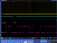
Below I generate 6 MCLK and 6 Trig pulse trains of 192 pulses using my SIS3610 module
s3610VFATclock(0,64575)
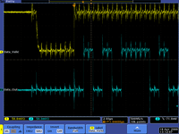
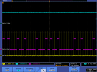
It appears above that the data valid pulse is only high for the first three pulses, like the LV1A trigger pulse? I thought it was suppose to be high during the entire data out pulse train.
4/18/09
I have given up trying to plug the VFAT card directly into the breakout box. If I plug the VFAT into a bread board and then into the Break out box then I can see data valid and data out pulses. The I2C communication works under either configuration.
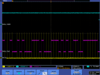
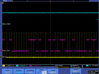
Below is a scope trace taken when I use LaTech Agilent pulser to generate a 1 KHz TTL pulse into the JLAB PLX board which outputs many LVDS copies. I then drive the VFAT with the JLAB PLX board LVDS output and look on the breakout box output pins at Data Valid and Data Out.
This may be compared to the original DF test pattern measured in Aug 2008.
As shown in the scope trace, the Data Valid pulse goes low to mark the end of the DF test pattern and the beginning of 2 idle pulses. The Data Valid pulse then goes high to mark the beginning of 192 DATAOUT pulses.
If I send this to my IO board I would expect to digital output to be
010101110100100001000101010?????????????????????????????????????????????????????????????????????????????????????????????????????
The first 12 bits are the bunch crossing number.
The next 12 bits are the event counter (EC) and Flags. 4 bits are used for the flag and 8 bits for the event counter.
Lets take snap shots of the pulse pattern using the scope to get the DF test pattern.
Bits 1-38
Bits 38-77
Bits 77-115
Bits 115-153
Bits 153-191
The next 12 bits are used for the chip ID. This will be related to the hex ID f3ee showing up via the I2C communication page with the chip. CHIPID(0) = f3 and CHIPID(1)=ee.
The next 128 bits are the hits on the 128 input channels to the chip.
The last 16 bits represent the checksum for the event block.
SIS3610 readout
- Design concept
- The SIS3610 will latch bits on a 16 bit IO connector for any given trigger. We will need to trigger and read the SIS3610 for each 194 pulses in the VFAT output pulse train. I will try to create a trigger pulse using the DATA VALID output pulse to form a logical and with the clock pulse. I will drive a gate generator with the MCLK signal and veto is with the DATA valid pulse.
LV1A
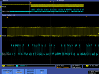
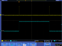
Scope pictures of the MCLK and LV1A pulses.
Has the LV1A pulse finished its transition in order to be latched by the Trigger Decoder Chip?
