Go Back to All Lab Reports
- RC Low-pass filter
1-50 kHz filter (20 pnts)
1. Design a low-pass RC filter with a break point between 1-50 kHz. The break point is the frequency at which the filter starts to attenuate the AC signal. For a Low pass filter, AC signals with a frequency above 1-50 kHz will start to be attenuated (not passed)
- To design low-pass RC filter I had:
[math]R=10.5\ \Omega[/math]
[math]C=1.250\ \mu F[/math]
[math]\omega_b = \frac{1}{RC} = 76.2\cdot 10^3\ \frac{rad}{s}[/math]
[math]f_b = \frac{\omega_b}{2\pi} = 12.1\ \mbox{kHz}[/math]
2. Now construct the circuit using a non-polar capacitor
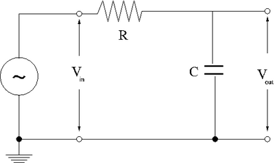
3. Use a sinusoidal variable frequency oscillator to provide an input voltage to your filter
4. Measure the input [math](V_{in})[/math] and output [math](V_{out})[/math] voltages for at least 8 different frequencies[math] (\nu)[/math] which span the frequency range from 1 Hz to 1 MHz
| [math]\nu\ [\mbox{kHz}][/math]
|
[math]V_{in}\ [V][/math]
|
[math]V_{out}\ [V][/math]
|
[math]\frac{V_{out}}{V_{in}}[/math]
|
[math]\nu\ [\mbox{kHz}][/math] |
[math]V_{in}\ [V][/math] |
[math]V_{out}\ [V][/math] |
[math]\frac{V_{out}}{V_{in}}[/math]
|
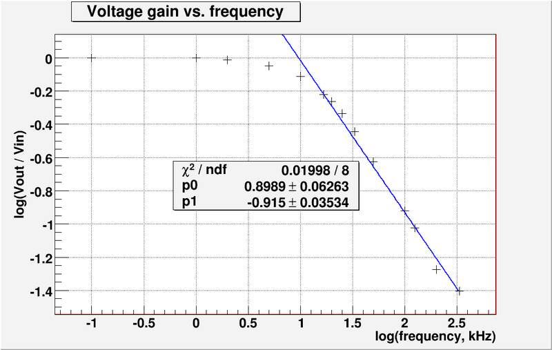
Table1. Voltage gain vs. frequency measurements
| 0.1 |
5.0 |
5.0 |
1.0
|
| 1.0 |
4.2 |
4.2 |
1.0
|
| 2.0 |
3.2 |
3.1 |
0.97
|
| 5.0 |
1.8 |
1.6 |
0.89
|
| 10.0 |
1.14 |
0.88 |
0.77
|
| 16.7 |
0.90 |
0.54 |
0.60
|
| 20.0 |
0.88 |
0.48 |
0.54
|
| 25.0 |
0.82 |
0.38 |
0.46
|
| 33.3 |
0.78 |
0.28 |
0.36
|
| 50.0 |
0.76 |
0.18 |
0.24
|
| 100.0 |
0.75 |
0.09 |
0.12
|
| 125.0 |
0.74 |
0.07 |
0.095
|
| 200.0 |
0.75 |
0.04 |
0.053
|
| 333.3 |
0.76 |
0.03 |
0.039
|
| 200.0 |
0.76 |
0.03 |
0.039
|
| 1000.0 |
0.78 |
0.06 |
0.077
|
5. Graph the [math]\log \left(\frac{V_{out}}{V_{in}} \right)[/math] -vs- [math]\log (\nu)[/math]
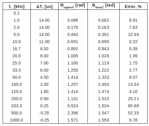
phase shift (10 pnts)
- measure the phase shift between [math]V_{in}[/math] and [math]V_{out}[/math] as a function of frequency [math]\nu[/math]. Hint: you could use [math] V_{in}[/math] as an external trigger and measure the time until [math]V_{out}[/math] reaches a max on the scope [math](\sin(\omega t + \phi) = \sin\left ( \omega\left [t + \frac{\phi}{\omega}\right]\right )= \sin\left ( \omega\left [t + \delta t \right] \right ))[/math].
See table above, columns #5 and #6.
Questions
1. Compare the theoretical and experimentally measured break frequencies. (5 pnts)
method 1. Using fitting line
- Theoretical break frequency: 12.1 kHz
- Experimentally measured break frequency: 9.59 kHz
 Q: The above was read off the graph?  Why not use fit results?
 A: The fit was made by using GIMP Image Editor. I do not have so much experience with ROOT. But I will try to do it. Thank you for comment.
 A1: The fit was done by ROOT
- The fit line equation from the plot above is [math]\ y=0.8989-0.915\cdot x[/math].
- From intersection point of line with x-axis we find:
- [math]log(f_{exp})=\frac{0.8989}{0.915} = 0.982[/math]
- [math]f_{exp} = 10^{0.982} = 9.59\ kHz [/math]
- The error is:
[math]Error = \left| \frac{f_{exp} - f_{theor}}{f_{theor}} \right| = \left| \frac{9.59 - 12.1}{12.1} \right|= 20.7\ %[/math]
method 2. Using the -3 dB point
At the break point the voltage gain is down by 3 dB relative to the gain of unity at zero frequency. So the value of [math]\mbox{log}(V_{out}/V_{in}) = (3/20) = 0.15 [/math]. Using this value I found from plot above [math]\mbox{log}(f_b) = 1.1\ \mbox{kHz}[/math]. So [math]f_b = (10^{1.1}) = 12.6\ \mbox{kHz}[/math]. The error in this case is 4.1 %.
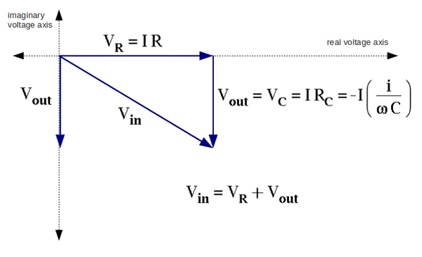
2. Calculate and expression for [math]\frac{V_{out}}{ V_{in}}[/math] as a function of [math]\nu[/math], [math]R[/math], and [math]C[/math]. The Gain is defined as the ratio of [math]V_{out}[/math] to [math]V_{in}[/math].(5 pnts)
We have:
- [math]1)\ V_{in} = I\left(R+R_C\right) = I\left(R+\frac{1}{i\omega C}\right)[/math]
- [math]2)\ V_{out} = I \left(\frac{1}{i\omega C}\right) [/math]
Dividing second equation into first one we get the voltage gain:
- [math]\ \frac{V_{out}}{V_{in}} = \frac{I \left(\frac{1}{i\omega C}\right)}{I\left(R+\frac{1}{i\omega C}\right)} = \frac{\left(\frac{1}{i\omega C}\right)}{\left(R+\frac{1}{i\omega C}\right)} = \frac{1}{1+i\omega RC}[/math]
And we are need the real part:
- [math]\left |\frac{V_{out}}{V_{in}} \right | = \sqrt{ \left( \frac{V_{out}}{V_{in}} \right)^* \left( \frac{V_{out}}{V_{in}} \right)} = \sqrt{\left ( \frac{1}{1+i\omega RC}\right ) \left ( \frac{1}{1-i\omega RC}\right )} = \frac{1}{\sqrt{(1 + (\omega RC)^2}} = \frac{1}{\sqrt{(1 + (2\pi \nu RC)^2}}[/math]
3. Sketch the phasor diagram for [math]V_{in}[/math],[math] V_{out}[/math], [math]V_{R}[/math], and [math]V_{C}[/math]. Put the current [math]I[/math] along the real voltage axis. (30 pnts)
4. Compare the theoretical and experimental value for the phase shift [math]\theta[/math]. (5 pnts)
The experimental phase shift is [math]\ \Theta_{exper} = (\omega\ \delta T)_{exper}[/math]
The theoretical phase shift is [math]\ \Theta_{theory}=\mbox{arctan}(\omega RC)[/math]
5. what is the phase shift [math]\theta[/math] for a DC input and a very-high frequency input?(5 pnts)
6. calculate and expression for the phase shift [math]\theta[/math] as a function of [math]\nu[/math], [math]R[/math], [math]C[/math] and graph [math]\theta[/math] -vs [math]\nu[/math]. (20 pnts)
Forest_Electronic_Instrumentation_and_Measurement
Go Back to All Lab Reports


