Difference between revisions of "Lab 17 RS"
| Line 84: | Line 84: | ||
[[File:L17 id vs vgs 21.png | 1000 px]] | [[File:L17 id vs vgs 21.png | 1000 px]] | ||
| + | |||
| + | |||
=5.) Calculate <math>y_{fs}</math> for your JFET (20 pnts)= | =5.) Calculate <math>y_{fs}</math> for your JFET (20 pnts)= | ||
| Line 92: | Line 94: | ||
So to calculate math>y_{fs}</math> we need to know function <math>I_D(V_{GS})</math>. Lets approximate this function by line: | So to calculate math>y_{fs}</math> we need to know function <math>I_D(V_{GS})</math>. Lets approximate this function by line: | ||
| + | |||
| + | [[File:L17 id vs vgs 22.png | 1000 px]] | ||
| + | |||
| + | As we can see from the plot above it is possible to approximate <math>I_D(V_{GS})</math> by line equation: | ||
| + | |||
| + | <math>I_D[mA] = (10.53 \pm 0.04)[mA] + (4.04 \pm 0.04)\ V_{GS}[V]</math> | ||
| + | |||
| + | and | ||
| + | |||
| + | <math>y_{fs} \equiv \left ( \frac{\partial I_D}{\partial V_{GS}} \right ) = \left ( \frac{\partial ((10.53 \pm 0.04)[mA] + (4.04 \pm 0.04)\ V_{GS}[V])}{\partial V_{GS}} \right )</math> = (4.04 \pm 0.04) | ||
| + | |||
=Question= | =Question= | ||
Revision as of 21:50, 10 April 2011
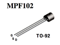
The JFET (Junction Field Effect Transistor n-channel)
File:JFET MPF102 DataSheet.pdf
1). Complete the table below for the JFET.
| Characteristic | Symbol | Min | Max | Unit |
| Zero-Gate-Voltage Drain Current | 2.0 | 20 | mAdc | |
| Gate-Source Cutoff Voltage | - | -8.0 | Vdc | |
| 3.3 M | ||||
| 1.0 M | ||||
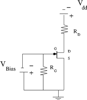
2.) Construct the JFET circuit below.
3.) Plot measurements of -vs- by varying for = 0, 0.5, 1.0, 1.5 V. (40 pnts)
I have used the following resistors:
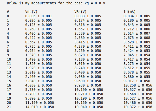
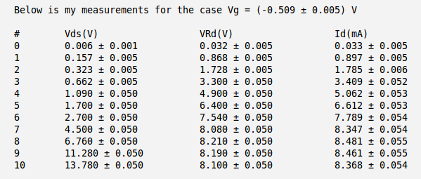
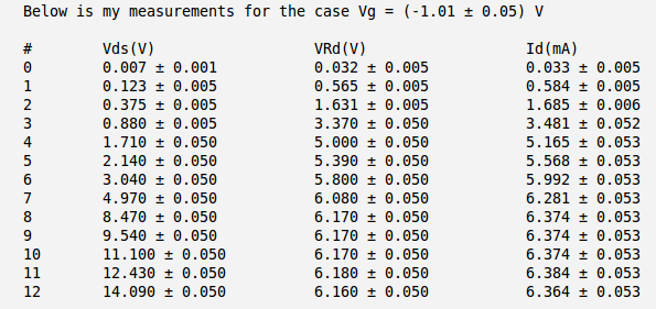
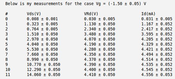
Below is the table with my measurements of voltages and and calculation of the current . Here I have used the meter to measure directly the voltage drop between the drain and source and to measure the voltage drop on resistor .
So my calculated current becomes:
.
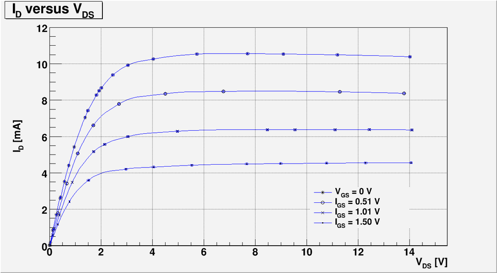
And below I have plotted four curves as function of for four different values of
4.) Plot -vs- (30 pnts)
For every measured values I have picked up the current values in the middle of saturation region of each line as follow:
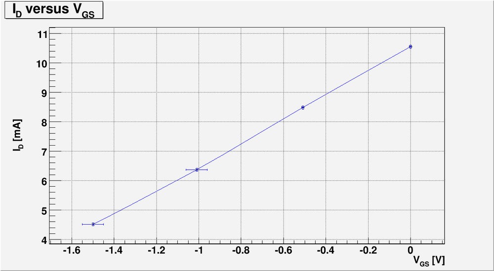
And below is my plot of -vs- :
5.) Calculate for your JFET (20 pnts)
For common source configuration JFET:
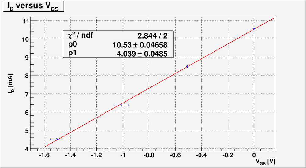
So to calculate math>y_{fs}</math> we need to know function . Lets approximate this function by line:
As we can see from the plot above it is possible to approximate by line equation:
and
= (4.04 \pm 0.04)
Question
Does depend on? (10 pnts)
Go Back to All Lab Reports Forest_Electronic_Instrumentation_and_Measurement
