Difference between revisions of "Lab 14 RS"
| Line 103: | Line 103: | ||
| − | Also note that my <math>V_{EC} = (11.32 \pm 0.01)\ V</math> is a little hire than my initial operating point <math>V_{EC} = 10\ V</math>. The main reason is that my actual values of <math>V_{BE} = (0.69 \pm 0.01)\ V </math> instead of <math>V_{BE} = 0.6\ V </math> as I was assumed initially. That will reduce my <math>V_C</math> voltage that reduce my <math>I_C</math> current. So I will shift right my operating point from <math>I_C = 5\ mA</math> to lower values and correspondingly will increase my <math>V_{EC}</math> | + | Also note that my <math>V_{EC} = (11.32 \pm 0.01)\ V</math> is a little hire than my initial operating point <math>V_{EC} = 10\ V</math>. The main reason is that my actual values of <math>V_{BE} = (0.69 \pm 0.01)\ V </math> instead of <math>V_{BE} = 0.6\ V </math> as I was assumed initially. That will reduce my <math>V_C</math> voltage that reduce my <math>I_C</math> current. So I will shift to right my operating point from <math>I_C = 5\ mA</math> to lower values and correspondingly will increase my <math>V_{EC}</math>. |
| − | + | ||
| + | But I still on my load line but my operating point now is <math>I_C = 4.26\ mA</math> and <math>V_{EC} = 11.32\ V</math> | ||
==Measure the voltage gain <math>A_v</math> as a function of frequency and compare to the theoretical value.(10 pnts)== | ==Measure the voltage gain <math>A_v</math> as a function of frequency and compare to the theoretical value.(10 pnts)== | ||
Revision as of 06:01, 20 March 2011
The Common Emitter Amplifier
Circuit
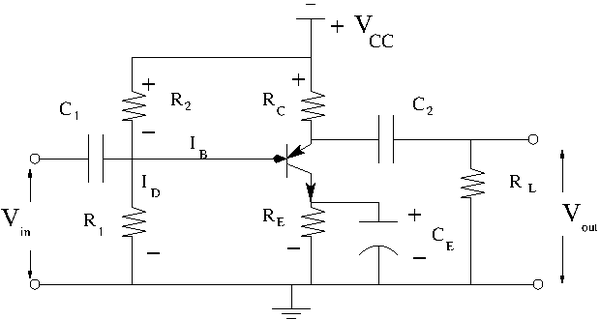
Construct the common emitter amplifier circuit below according to your type of emitter.
Calculate all the R and C values to use in the circuit such that
- a. Try and
- b. mA DC with no input signal
- c. V
- d. to prevent burnout
- e.
- f. mA
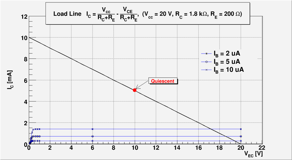
Let's , and . The load line equation becomes:
This load line pretty high and give me the wide range of amplification the input signal.
Draw a load line using the -vs- from the previous lab 13. Record the value of or .
On the plot above I overlay me output lines from the previous lab report #13 and me load line I am going to use to construct amplifier. My based on my previous lab report #13
Set a DC operating point so it will amplify the input pulse given to you. Some of you will have sinusoidal pulses others will have positive or negative only pulses.
I will set up my operating point in the middle of the load line: , . So I will have the wide range of amplification the input signal
Let's calculate all bias voltage to set up this operating point.
So to get this operating point I need to set up . I can do it using voltage divider . To get operating point independent of the transistor base current we want
.
Here are have used instead of as in my previous lab because it's my actual values of here. I have measured this using millivoltmeter.
Let's
So
And we can find using the voltage divider formula
So
Let's check it:
as should be.
Measure all DC voltages in the circuit and compare with the predicted values.(10 pnts)
My predicted DC voltage are:
We have from operating point:
And because we have silicon transistor:
Now
My measured DC voltage are:
First note that my is close to predicted values .
Also note that my is a little hire than my initial operating point . The main reason is that my actual values of instead of as I was assumed initially. That will reduce my voltage that reduce my current. So I will shift to right my operating point from to lower values and correspondingly will increase my .
But I still on my load line but my operating point now is and
Measure the voltage gain as a function of frequency and compare to the theoretical value.(10 pnts)
Measure and at about 1 kHz and compare to the theoretical value.(10 pnts)
How do you do this? Add resistor in front of which you vary to determine and then do a similar thing for except the variable reistor goes from to ground.
Measure and as a function of frequency with removed.(10 pnts)
Questions
- Why does a flat load line produce a high voltage gain and a steep load line a high current gain? (10 pnts)
- What would be a good operating point an an common emitter amplifier used to amplify negative pulses?(10 pnts)
- What will the values of , , and be if the transistor burns out resulting in infinite resistance. Check with measurement.(10 pnts)
- What will the values of , , and be if the transistor burns out resulting in near ZERO resistance (ie short). Check with measurement.(10 pnts)
- Predict the change in the value of if is increased from 10 to 50 (10 pnts)
- Sketch the AC equivalent circuit of the common emitter amplifier.(10 pnts)
Go Back to All Lab Reports Forest_Electronic_Instrumentation_and_Measurement

