Difference between revisions of "Interim Report 5-18-08 AwardNum0653570"
| Line 74: | Line 74: | ||
====Speed test results==== | ====Speed test results==== | ||
| + | The VFAT is a candidate front end readout card for Qweak's region 1 tracking system. The VFAT chip has been designed to sample the detector analog output at 40 MHz. Although elastically scattered electrons which traverse the entire Qweak apparatus are expected to trigger the readout system at rates of about 1 kHz, there is a large background due to moller scattering which corresponds to rates of 12 MHz/nA uniformly distributed over the entire region 1 acceptance. The moller rate on a single detector strip would be about 25 kHz/nA. This restricts the region 1 tracking system to operating currents below 400 nA since the detector rise time of 50 nanoseconds will result in signal pileup if the ionization particle flux rates exceed 10 MHz. The VFAT board by itself can satisfy the readout requirements of Qweak. | ||
| − | The | + | The remaining question is whether the transfer of the VFAT digital output to the data acquisition system without introducing a bottleneck. The CERN engineer who designed the VFAT board suggested the use of a Field Programmable Gate Array (FPGA). THE VME 1495 FPGA I/O module from CAEN was selected for testing. We observed read and write speeds between the VME backplane and the FPGA user registers of 16 bits to USER FPGA in 330 ns. This measurement correspond to a throughput speed of 6 MB/sec compared to a requirement of 0.5 kb/sec for Qweak. |
| − | |||
| − | |||
| − | |||
| − | |||
==== VFAT communication protocols==== | ==== VFAT communication protocols==== | ||
Revision as of 16:46, 13 July 2008
Participants
		Tony Forest	   Principal Investigator	Yes
		Julian Salamanca	   Graduate student	No
		Tamar Didberidze	   Graduate student	Yes
		Jordan Keough	   Undergraduate student	No
		Jeremy Lebaron	   Undergraduate student	Yes
Activities and Findings
This section will serve as your report to your program officer of your project's activities and findings. Please describe what you have done and what you have learned, broken down into four categories:
What have been your major research and education activities (experiments, observations, simulations,presentations, etc.)
The construction of the Region 1 tracking system for the Qweak experiment has been the main research focus of the support from this proposal. The Qweak experiment is scheduled to measure the parity violating elastic scattering of polarized electrons from protons at Jefferson Lab. The measurement will be used to extract the weak mixing angle and thereby test the standard model. The PI for this award is responsible for the design and construction of the Region 1 detector system. Other activities also undertaken include the testing of prototype drift chambers for the Hall-B 12 GeV upgrade and an analysis of experimental data which will lead towards the extraction of nucleon polarized structure functions. The progress of these endeavors is described below.
Qweak Region 1 Tracking System Detector Construction
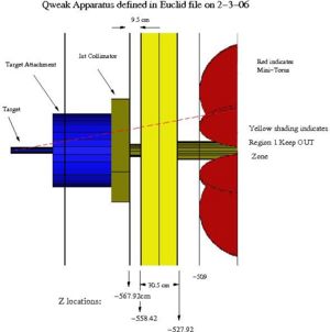
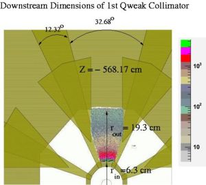
The design, construction, and testing of the Region 1 tracking system for the Qweak experiment at Jefferson Lab has been the main research activity supported by this grant. The Qweak Region 1 tracking system is one of three tracking systems designed to measure the profile of elastically scattered electrons as well as background contributions to the parity violating signal. The Region 1 tracking system is located behind the first collimator at a distance of about 550 cm from the main torus magnet ( 200 cm from the target) as show in the left hand figure below. The collimator divides the acceptance into 8 regions, octants, and reduces the azimuthal acceptance by almost 30 percent. The right hand figure below shows the elastic scattering profile overlayed on top of one of the octants. The Region 1 tracking system will measure the electron scattering angle at only 2 of the octants at a time and will rotate in to perform measurements in the remaining octants.
The high radiation flux and the small detector footprint are two of the biggest challenges facing the Region 1 tracking system. An ionization chamber equipped with Gas Electron Multipliers (GEM) was chosen in order to accommodate the high radiation flux near the target. The GEM preamplifiers allow smaller ionization cell sizes thereby resulting in ionization chamber rise times of 50 nanoseconds or less. The ionization chamber itself is constructed from Ertalyte, a machinable plastic material which can withstand the high radiation environment. The material's strength allows the chamber to have thin walls which prevent the chamber from extending into adjacent octants. The three major components to the Qweak Region 1 detector are the GEM preamplifiers, the charge collector, and the ionization chamber are describe below.
Preamplifier design and procurement
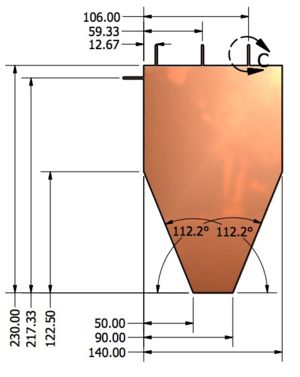
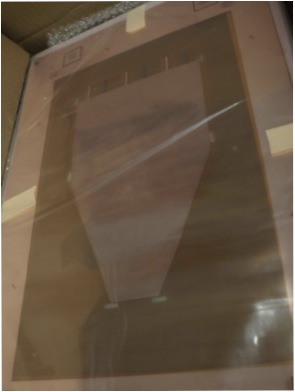
The figure below shows the custom designed GEM preamplifier for the Qweak Region 1 tracking system. The preamplifier is a 50 micron thick kapton foil clad on both sides with 5 microns of copper. Holes are etched into the foil such that a high voltage (HV) applied across the top and bottom copper plates will create an electric field strong enough to cause charge to pass through the hole and multiply much like the avalanche region of a drift chamber. Engineers from the Idaho Accelerator Center (IAC) designed the shape of the foils and the location of 6 tabs used for HV connections, as shown in the left hand figure below. This generic design allows one to use the part for any GEM amplification stage simply by cutting off the unused HV tabs. The actual preamp is shown on the right hand side of the figure below. Although this is a simple part, it is a clear example of how the infrastructure at the IAC can be leveraged in support of our physics mission.
Charge Collector Design
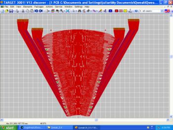
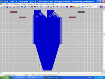
The charge collector for Qweak's region 1 tracking system is shown below. The copper charge collector strips are aligned in terms of the electron scattering angle . Each of the red strips shown in the right hand figure below is 400 microns wide and will measure the elastic electron scattering angle to within 0.1 mrad. The blue lines shown in the left hand figure are representative of the scattering angle. A large number of graduate student hours were needed to place each strip into the correct position using PC board design software. Software compatibility issues with the vendor were also a major time sink of several months before the part could be accurately manufactured according to our specifications. This single part represents the bulk of a graduate students effort for the past 6 months and is one example of a practical component to a students educational experience. The vendor is currently fabricating the part and is expected to arrive by the end of July, 2008.
Ionization Chamber Construction
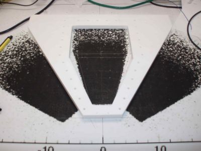
The ionization chamber for the Qweak Region 1 tracking system needs to have a small profile in order to be placed less than a quarter meter after the target. A collimator in front of this detector divides the electron scattering anglular range into octants which reduce the angular acceptance range by about 30 percent. The goal was to construct a chamber which did not interfere with the other octants and be transportable between octants. The figure below shows the top half of the ionization chamber which has been built. As seen in the figure, the electron profile is enclosed by the detector acceptance and the ionization chamber frame is in the shadow of the collimator. The HV distribution board has been designed by physics undergraduate student Jordan Keough and is ready to be sent out for production. Chamber construction will be completed when the charge collector arrives from the vendor and is installed. We expect to test the chamber in August, 2008.
Qweak readout electronics
The front end readout electronics for Qweak's region 1 tracking system will need to withstand the high radiation environment as well as have a fast throughput. One detector readout option being pursed is the VFAT digitization board developed at CERN for the TOTEM experiment. It was designed to be used for either silicon or GEM based detectors. The board can sample it's 128 input channels at 40 MHz and store up to 128 triggered events. The VFAT board has been designed to withstand up to 100 Mrad of radiation which is more than sufficient for Qweak. The VFAT card digitizes the analog output of the GEM detector to indicate the presence of a hit on one of the charge collector's copper strips. The PI has been using his start up funds to develop the infrastructure needed to deploy this front end electronics for the Qweak's region 1 tracking system. This infrastructure is described below.
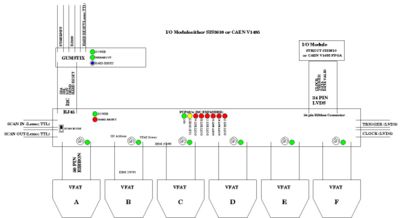
The front end electronics to readout a detector contains three basic elements. The VFAT readout board will convert the analog charge observed on a charge collector strip to a digital signal which identifies the presence of a hit on the strip. A Gumstick controller is a small unix computer used to program the VFAT card and set parameters like the amplifier gain, the threshold, and check for failed flip/flops. A VME I/O board will receive the LVDS digital signals from the VFAT board and store them for readout by a single board computer located in the VME crate. For the past year, Brian Oborn has been working on the Gumstick controller to communicate with a VFAT board. Undergraduate student, Jordan Keough, is spending the summer designing a signal switchyard to establish lines of communication between the Gumstick computer, the VFAT board, and the VME I/O module.
VFAT board communication
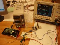
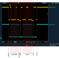
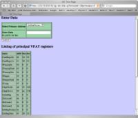
The figure below illustrates the progress which has taken place developing the VFAT readout infrastructure. The first image illustrates a test setup showing the VFAT chip output viewed by an oscilloscope during our signal tests. The second image is a scope picture iidentifying the LVDS communication protocols when we program the chip. The last image shows a web interface we are using to program the chip. The Gumstick computer has a webserver loaded which will allow a web browser to set VFAT parameters remotely from the counting house at JLAB.
Readout switchyard
The lines of communication between the VFAT readout board, the Gumstick controller, and the VME FPGA I/O module are managed by a signal switchyard being designed at ISU. Brian Oborn, a technician from the IAC, is mentoring Jordan Keough's design of the signal switchyard board. Jordan is a physics undergraduate. The switchyard will divert signals between the three detector readout elements to their appropriate destination. I2C signals will travel between the Gum stick control computer to the VFAT readout card according to address switches on the switchyard board. The switchyard board will also be used to input clock signals for sampling the detector as well as a Flip Flop scan signal to check for radiation damage to the board. The switchyard will send LVDS signals containing the Detector data from the VFAT readout board to the VME FPGA I/O module.
Physics Analysis
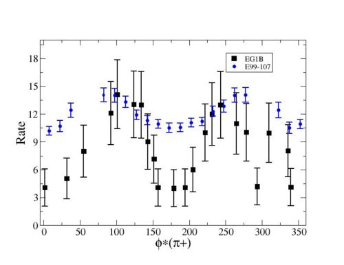
While the construction and testing of ionization chambers for Qweak is a valuable graduate student hardware experience, the graduate student supported by this grant will need to write a thesis on a research physics topic. Due to the time constraints involved, Tamar Didberidze, has been doing her physics research on data that has already been taken. She has decided to work towards measuring the ratio of polarized to unpolarized down quark distribution in the nucleon. The PI's previous work at JLAB involved collecting polarized electron scattering data from polarized ammonia targets using the CLAS. Tamar will be able to analyze the polarized structure function data already taken and not wait for data from the Qweak experiment in order to graduate from with a Ph. D. in a timescale consistent with such a degree. Preliminary results from her analysis are shown in the next section.
What are your major findings from the activities identified above
Qweak readout electronics
Speed test results
The VFAT is a candidate front end readout card for Qweak's region 1 tracking system. The VFAT chip has been designed to sample the detector analog output at 40 MHz. Although elastically scattered electrons which traverse the entire Qweak apparatus are expected to trigger the readout system at rates of about 1 kHz, there is a large background due to moller scattering which corresponds to rates of 12 MHz/nA uniformly distributed over the entire region 1 acceptance. The moller rate on a single detector strip would be about 25 kHz/nA. This restricts the region 1 tracking system to operating currents below 400 nA since the detector rise time of 50 nanoseconds will result in signal pileup if the ionization particle flux rates exceed 10 MHz. The VFAT board by itself can satisfy the readout requirements of Qweak.
The remaining question is whether the transfer of the VFAT digital output to the data acquisition system without introducing a bottleneck. The CERN engineer who designed the VFAT board suggested the use of a Field Programmable Gate Array (FPGA). THE VME 1495 FPGA I/O module from CAEN was selected for testing. We observed read and write speeds between the VME backplane and the FPGA user registers of 16 bits to USER FPGA in 330 ns. This measurement correspond to a throughput speed of 6 MB/sec compared to a requirement of 0.5 kb/sec for Qweak.
VFAT communication protocols
Cuts: EC_inner>0.06, EC_tot/p>0.2, nphe>2.5, , and .
What research and teaching skills and experience has the project helped provide to those who worked on the project
Describe the opportunities for training and development provided by your project.
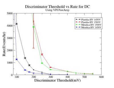
As part of her graduate studies, Tamar Didberidze has been quantifying the performance of two proto-type drift chambers for Hall-B. The ionization chamber principle is similar to the GEM chambers being built for Qweak. Two ionization chamber proto-types were built by JLab and sent to ISU. They are identical except that one uses an all plastic feedthrough to hold the drift chamber wires and another has a plastic feedthrough with a metal tip where the wire makes contact with the feedthrough. The proto-type detectors will be used to evaluate the efficency of the chamber as a function of the ionizating particles position from the end of the wire. A Garfield simulation leads one to believe that the plastic tipped feedthrough will result in a less efficent detector near the end of the wire due to a less radial electric field lines. The answer to this question will impact the design of drift chambers for the CLAS 12 upgrade.
During this funding cycle, Tamar has discovered that the proto-type detector using plastic feedthroughs is noisier than the one which has metal tips.
As part of his graduate student studies, Julian Slamanca has gained substantial experience machining the Qweak detectors.
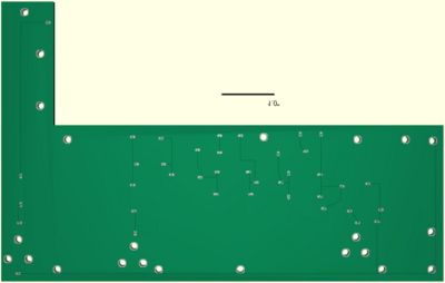
Julian Salamance and Jordan Kenough gained experience designing circuit boards. Julian design the charge collector for Qweak which is being fabricated by CERN. Jordan design the HV distribution board which was described above.
What outreach activities have you undertaken to increase public understanding of, and participation in, science and technology?
Describe outreach activities your project has undertaken.
The physics department at ISU travels to local schools to perform physics demonstrations in an effort to increase the publics understanding of science and technology. The demonstrations occur at night in order to illustrate physics principles to students and their parents. I went to Syringa elementary school during this last funding cycle to demonstrate several principles of electricity to student and their parents. A small Van de Graf was used to demonstrate principles of conduction. The principles of producting electricity were demonstrated using solenoids and the effect of liquid nitrogen on Eddy currents induced in a copper conducter were some of the popular components of the demonstrations.
The physics department also holds a mentoring program for high school teachers and their students during the first month of summer. I instructed as group of about 20 teachers and student on the operating principles of drift chambers, scintillators, and solid state detectors. He-3 neutron detectors will be given to the science teachers for use at their home institution. As a result, the neutron detection principle of a He-3 detector was the main focus of the lecture. The He-3 detectors are from a completed experiment at PNNL laboratories and were made available to ISU's due to its research partnership with PNNL Laboratories. The arrangement is a fortuitous example of how research and education can combine forces to improve the publication understanding of science and technology.
Publications and Products
In this section, you will be asked to describe the tangible products coming out of your project. Specifically:
What have you published as a result of this work? Journal publications
Books or other non-periodical, one-time publications
What Web site or other Internet site have you created?
What other specific products (databases, physical collections, educational aids, software, instruments, or the like) have you developed?
What have you published as a result of this work?
This work is in progress and has not resulted in any publications.
Journal publications
Books or other non-periodical, one-time publications
What Web site or other Internet site have you created?
Wiki
What other specific products (databases, physical collections, educational aids, software, instruments, or the like) have you developed?
Contributions
Now we invite you to explain ways in which your work, your findings, and specific products of your project are significant. Describe the unique contributions, major accomplishments, innovations and successes of your project relative to :
the principal discipline(s) of the project;
other disciplines of science or engineering;
the development of human resources;
the physical, institutional, or information resources that form the infrastructure for research and education; and
other aspects of public welfare beyond science and engineering, such as commercial technology, the economy, cost-efficient environmental protection, or solutions to social problems.
