Detector Description
GEM Detector Design and Structure
The GEM preamplifier described in section XXXX was used to increase the signal amplitude of the ionization chamber. Primary electrons are liberated by an ionizing particle intersecting an ionization chamber that has a 90/10 Ar/CO2 gas; the cathode's electric field accelerates the electrons towards the GEM preamplifier. As described in section XXX, a single GEM preamplifier can increase the number of liberated electron by three orders of magnitude via secondary ionization.<ref = "chechik"> R. Chechik, A. Breskin, G. P. Guedes, D. Mörmann, J. M. Maia, V. Dangendorf, D. Vartsky, J. M. F. Dos Santos, and J. F. C. A. Veloso, Recent Investigations of Cascaded GEM and MHSP detectors, IEEE Trans. Nucl. Sci. 2004 </ref> Using three pre-amplifiers will increase the signal amplitude making it measurable. A high voltage divider circuit is used to establish the electric fields for each preamplifier using a single power supply channel, and secondary electrons are guided towards a segmented charge collector.
Detector Structure
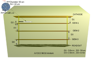
The triple GEM detector is composed of three GEM preamplifiers, a cathode and an anode. A GEM preamplifier is a 50 micron thick kapton foil clad on both sides with 5 microns of copper. A staggered pattern of 50 micron diameter holes, equally spaced by distances comparable to the hole diameter, is chemically etched into the copper clad foil of a 140 um pitch distance over an area of 10x10cm. <ref name = "Souli"> F. Sauli, et al, NIM A 386, 531 (1997) </ref> The detector contains three GEM preamplifiers mounted on square plastic frames separated by a vertical distance of 2.8 mm and placed parallel to the cathode as shown in the figure below.
The cathode is a square copper plate that is 10x10cm and is 3.5 mm away from the top of the first GEM card. This cathode design is capable of being set to be at a potential voltage of 5 kV (in the air) without any discharge. The charge collector (readout anode) is constructed of 50-80 micron wide strips that are insulated to determine the location of the collected electrons, and are arranged to allow equal charge sharing on the upper (x coordinate) and lower (y coordinate) charge collector layers <ref name= readout>Physik Department E18, Technische University Munchen, 2D readout Plane, 21 of Jun.2012. http://www.e18.ph.tum.de/research/compass/gempixelgem-tracking-detectors </ref>.
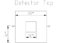
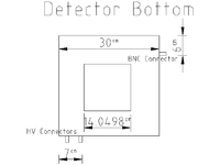
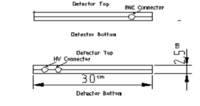
All the above components exist in a sealed chamber that consists of two ertalyte plastic sheets; they are bolted together by a number of M3 plastic screws located around the detector window to form a well enclosed cavity. Also, the chamber has a 13x13cm kapton window to reduce the energy loss of incident particles entering the chamber. The figures below show top, bottom, and side views of the detector's chamber design.
Modifying the GEM detector as neutron sensitive detector
The GEM’s original design was modified to convert it to a neutron-sensitive detector. As mentioned previously in Section YYY, fissionable material, inserted inside the chamber, may be used to indirectly detect neutrons by detecting the ionization caused by fission fragments released into the chamber if a neutron induced fission event occurs. The cathode design has a 3 cm diameter coating of U-233 with a 30-40 um thickness. The kapton window height was increased 2.5 mm to accommodate an increase in the distance of the cathode to 8 mm from the top of the first of GEM card (instead of 3.5 mm in the original design). An FR4 shutter which had enough area to cover the fissionable material was attached in the space between the cathode and the first GEM card. The shutter could be opened or closed from outside the chamber. When the shutter is closed, it covers the U-233 coating and stops the emitted fission fragments ionizing the gas beyond the shutter. When the shutter is open, the ionization due to fission fragments produces a signal.
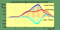
The shutter has the ability to stop the fission fragments that are emitted from U-233 coating. Having the U-233 as a source for alpha particles, the QDC charge spectrum showed a difference in case the shutter was open and when it was close, such a test proved the ability of the FR4 shutter to stop (or partially stop) the emitted alpha particles from U-233 coating. The figure below shows the charge spectra in case of shutter open and closed as the detector's operating voltage is 2.6 kV and 2.9 kV for GEM and cathode successively.
Since the fission fragments are heavier ions than the alpha particles, a closed shutter should stop them. Such an ability is important to distinguish the fission fragments' signal from the other particles' signals in a heavy radiation environment created in an operating accelerator or a reactor.
What about alpha and beta particles.
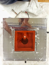
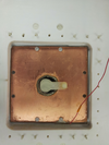
The figures below show the modified components of the detector.
High voltage divider circuit
The GEM preamplifiers are connected with high voltage divider circuit that determines the electron multiplication and transfer to the readout plate. The GEM cards are connected to the high voltage divider circuit that is shown in the figure below:

It provides the cathode with a voltage of 3.6 kV, and it produces an electric field which drifts most of the electrons that are primarily produced by ionization. The circuit also provides the GEM preamplifiers with voltage between the top and bottom of each card; the voltage gradually decreases to have the least value between the sides of the third GEM card. This design's advantage is to provide enough voltage for electron multiplication, and to guide most of the drift electrons to the grounded readout plate.
The following table shows the voltage measurements between the sides of the GEM preamplifiers, and voltage between each side and the ground using the HV-voltage divider circuit shown in figure (2).
| 2550 | 2579 | 2259 | 304 | 1671 | 1394 | 279 | 818 | 570 | 245 |
| 2600 | 2630 | 2303 | 310 | 1704 | 1421 | 285 | 834 | 581 | 250 |
| 2650 | 2680 | 2348 | 316 | 1737 | 1449 | 290 | 850 | 592 | 255 |
| 2700 | 2731 | 2393 | 322 | 1770 | 1476 | 296 | 866 | 603 | 260 |
| 2750 | 2781 | 2373 | 328 | 1803 | 1503 | 302 | 882 | 614 | 264 |
| 2800 | 2832 | 2482 | 332 | 1836 | 1530 | 307 | 898 | 625 | 269 |
<references/>
Go Back [1]
