Charge Collector Design
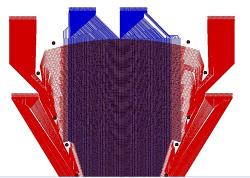
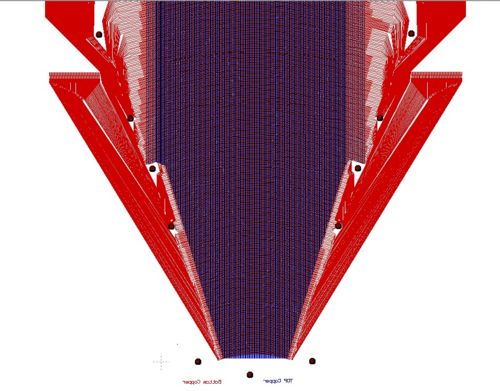
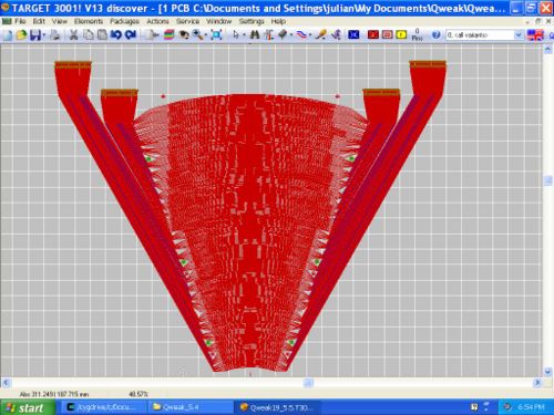
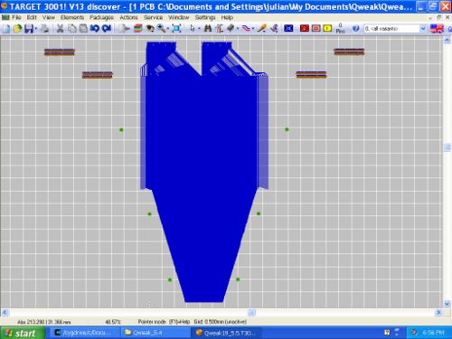
The charge collector for the Qweak chambers will use concentric strips aligned with the electron scattering polar angle (: the Z-axis is pointing along the beam direction), shown as the top layer below in read, and radial strips (shown as the bottom layer in blue). The radial strip are not aligned with phi due to the expected phi symmetry. Six, 130 pin output connectors will be used. Two of the pins are ground and 128 carry signals from individual strips. The PCboard design oftware had trouble displaying the entire readout board at once such that you could see enough detail. The two pictures below represent the Top and Bottom halfs of the readout board. A view of the entire board can be seen using a Gerber file viewer. The picture of the top and Bottom layers can be found here ReadoutBoardGerberFiles along with links to the gerber files themselves.
The Top Half of the Charge Collector showing all six output conenctors
This is the bottom half of the charge collector showing only the bottom 2 output connectors
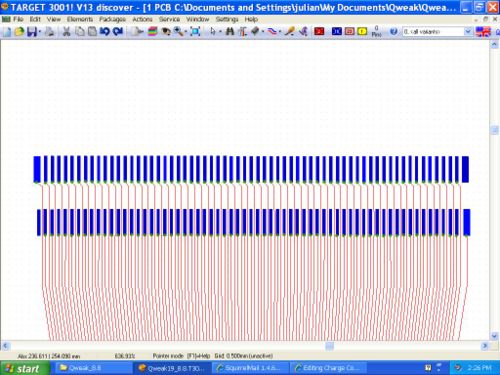
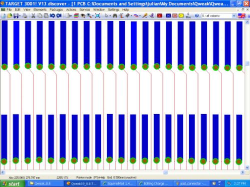
A close up view of the 130 pin pads which will be used to mount connectors for the VFAT cards.
We need to have plated holes which allow the copper lines to pass through to the very last layer where the copper pads for the 130 pin connector are.
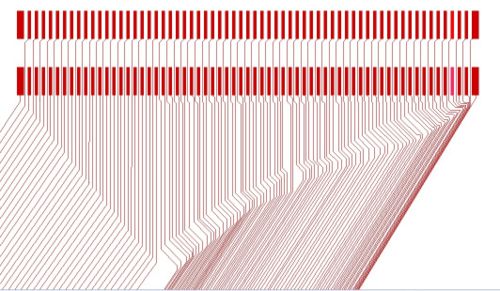
The main web page for the connectors is at
[1]
Taget3001_GerberFileProblem Target 3001 design software
Latest Design 12/07
Bottom Copper Layer
Internal radius: 69.7mm
External radius: 313.9mm
Circular lines width: 0.4mm
Top Copper Layer
line width: 0.1mm
