Difference between revisions of "Breakout Board Design"
Jump to navigation
Jump to search
| (2 intermediate revisions by the same user not shown) | |||
| Line 1: | Line 1: | ||
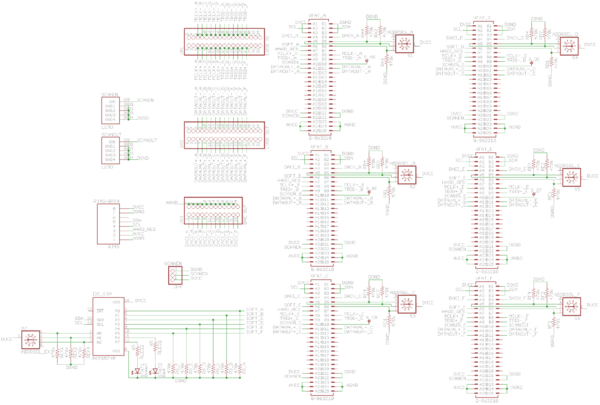
| − | This is the current schematic for the connections on the breakout board | + | This is the current schematic for the connections on the breakout board: |
[[Image:Breakout Board Schematic 1.png | 600px]] | [[Image:Breakout Board Schematic 1.png | 600px]] | ||
| − | + | The board, top and bottom layers only: | |
| − | + | [[Media:VFAT_breakout_top_bot.pdf]] | |
| − | + | ||
| − | + | The board, middle layers only: | |
| − | + | [[Media:VFAT_breakout_middle.pdf]] | |
| + | |||
| + | The board: all layers: | ||
| + | [[Media:VFAT_breakout_all.pdf]] | ||
| + | |||
| + | |||
| + | width = 110 mm | ||
| + | |||
| + | length =184 mm | ||
[[Old Breakout Board Design]] | [[Old Breakout Board Design]] | ||
Latest revision as of 19:15, 16 September 2009
This is the current schematic for the connections on the breakout board:
The board, top and bottom layers only: Media:VFAT_breakout_top_bot.pdf
The board, middle layers only: Media:VFAT_breakout_middle.pdf
The board: all layers: Media:VFAT_breakout_all.pdf
width = 110 mm
length =184 mm
