Lab 13 RS

From New IAC Wiki
Revision as of 04:07, 22 March 2011 by Shaproma (talk | contribs) (→‎Extra credit)
(diff) ← Older revision | Latest revision (diff) | Newer revision → (diff)
Jump to navigation Jump to search

Go Back to All Lab Reports


DC Bipolar Transistor Curves

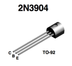
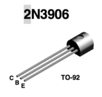
Data sheet for transistors.

Media:2N3904.pdf Media:2N3906.pdf

2N3904 PinOuts.png2N3906 PinOuts.png


Using 2N3904 is more srtaight forward in this lab.

Transistor circuit

1.) Identify the type (n-p-n or p-n-p) of transistor you are using and fill in the following specifications.


I am going to use n-p-n transistor 2N3904. Below are some specifications from data shits for this type of transistor:

Value Description
[math]V_{(BR)CEO} = 40\ V[/math] Collector-Base breakdown voltage
[math]V_{(BR)EBO} = 6\ V[/math] Emitter-Base Breakdown Voltage
[math]V_{(BR)CEO} = 40\ V[/math] Maximum Collector-Emitter Voltage
[math]V_{(BR)CBO} = 60\ V[/math] Maximum Collector-Emitter Voltage
[math]I_C = 200\ mA[/math] Maximum Collector Current - Continuous
[math]P = 625\ mW[/math] Transistor Power rating([math]P_{Max}[/math])
[math]h_{FE}\ min \ [/math] [math]h_{FE}\ max \ [/math] [math]I_C[/math], [math]V_{CE}[/math]
40 300 [math]I_C=0.1\ mA[/math], [math]V_{CE}=1.0\ V[/math]
70 300 [math]I_C=1\ mA[/math], [math]V_{CE}=1.0\ V[/math]
100 300 [math]I_C=10\ mA[/math], [math]V_{CE}=1.0\ V[/math]
60 300 [math]I_C=50\ mA[/math], [math]V_{CE}=1.0\ V[/math]
30 300 [math]I_C=100\ mA[/math], [math]V_{CE}=1.0\ V[/math]


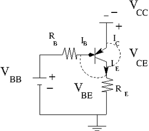
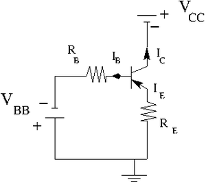
2.) Construct the circuit below according to the type of transistor you have.

TF EIM Lab13a Circuit.pngTF EIM Lab13 Circuit.png


Let [math]R_E = 100 \Omega[/math].

[math]V_{CC} \lt 5 Volts[/math] variable power supply

[math]V_{BE}= 1\ V[/math].

Find the resistors you need to have

[math]I_B = 2 \mu A[/math] , [math]5 \mu A[/math] , and [math]10 \mu A[/math]

By measurements I was able to find that [math]V_{BE}= 0.6\ V[/math]. So I am going to use this value. Also let picks up [math]V_{BB}= 1.6\ V[/math]. So my current [math]I_B = \frac{V_{BB} - V_{BE}}{R_B} = \frac{(1.6 - 0.6)\ V}{R_B} = \frac{1.0\ V}{R_B}[/math].

Now to get [math]I_B = 2\ \mu A[/math] I need to use [math]R_B = \frac{1.0\ V}{2\ \mu A} = 500\ k\Omega[/math]
    To get [math]I_B = 5\ \mu A[/math] I need to use [math]R_B = \frac{1.0\ V}{5\ \mu A} = 200\ k\Omega[/math]
    To get [math]I_B = 10\ \mu A[/math] I need to use [math]R_B = \frac{1.0\ V}{10\ \mu A} = 100\ k\Omega[/math]


3.) Measure the emitter current [math]I_E[/math] for several values of [math]V_{CE}[/math] by changing [math]V_{CC}[/math] such that the base current [math]I_B = 2 \mu[/math] A is constant. [math]I_B \approx \frac{V_{BB}-V_{BE}}{R_B}[/math]


I used:

[math]R_1 = (199.5 \pm 1.0)\ k\Omega [/math]
[math]R_1 = (198.7 \pm 1.0)\ k\Omega [/math]
[math]R_1 = (100.0 \pm 1.0)\ k\Omega [/math]
[math]R_B = (R_1 + R_2 + R_3) = (498.2 \pm 1.7)\ k\Omega [/math]

and

[math]R_E = (100.0 \pm 1.0)\ \Omega [/math]


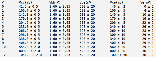
Below is the table with my measurements:

Table 2uA 01 corrected.png


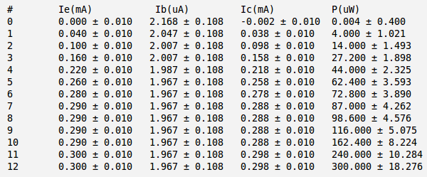
And below is my currents and power calculation:

Here:

[math]I_{E} = \frac{V_E}{R_E}[/math]
[math]I_{B} \approx \frac{V_{BB}-V_{BE}}{R_B}[/math]
[math]P_{max} = I_C \cdot V_{CE} = (I_E - I_B) \cdot V_{CE} [/math] 

and I have used approximation [math]V_{E} \approx o[/math]


Table 2uA 02 corrected.png


4a.) Repeat the previous measurements for [math]I_B \approx 5\ \mu A[/math]. Remember to keep [math]I_CV_{CE} \lt P_{max}[/math] so the transistor doesn't burn out


I used:

[math]R_B = (199.5 \pm 1.0)\ k\Omega [/math]

and

[math]R_E = (100.0 \pm 1.0)\ \Omega [/math]


Below is the table with my measurements:

Table 5uA 01 corrected.png


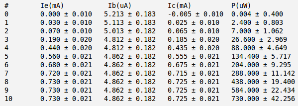
And below is my currents and power calculation:

Here:

[math]I_{E} = \frac{V_E}{R_E}[/math]
[math]I_{B} \approx \frac{V_{BB}-V_{BE}}{R_B}[/math]
[math]P_{max} = I_C \cdot V_{CE} = (I_E - I_B) \cdot V_{CE} [/math] 

and I have used approximation [math]V_{E} \approx o[/math]


Table 5uA 02 corrected.png


4a.) Repeat the previous measurements for [math]I_B \approx\ 10 \mu A[/math]. Remember to keep [math]I_CV_{CE} \lt P_{max}[/math] so the transistor doesn't burn out


I used:

[math]R_B = (100.0 \pm 1.0)\ k\Omega [/math]

and

[math]R_E = (100.0 \pm 1.0)\ \Omega [/math]


Below is the table with my measurements:

Table 10uA 01 corrected.png


And below is my currents and power calculation:

Here:

[math]I_{E} = \frac{V_E}{R_E}[/math]
[math]I_{B} \approx \frac{V_{BB}-V_{BE}}{R_B}[/math]
[math]P_{max} = I_C \cdot V_{CE} = (I_E - I_B) \cdot V_{CE} [/math] 

and I have used approximation [math]V_{E} \approx o[/math]


Table 10uA 02 corrected.png


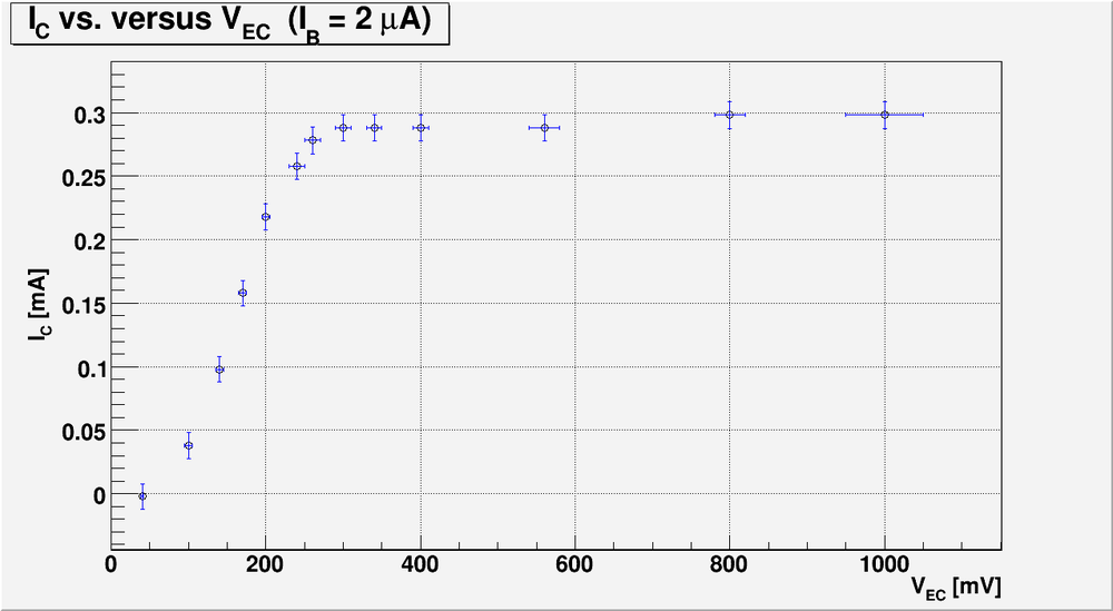
5.) Graph [math]I_C[/math] -vs- [math]V_{CE}[/math] for each value of [math]I_B[/math] and [math]V_{CC}[/math] above. (40 pnts)

Bellow is my plot for the case of [math]I_B = 2 \mu A[/math]

Plot 2uA.png


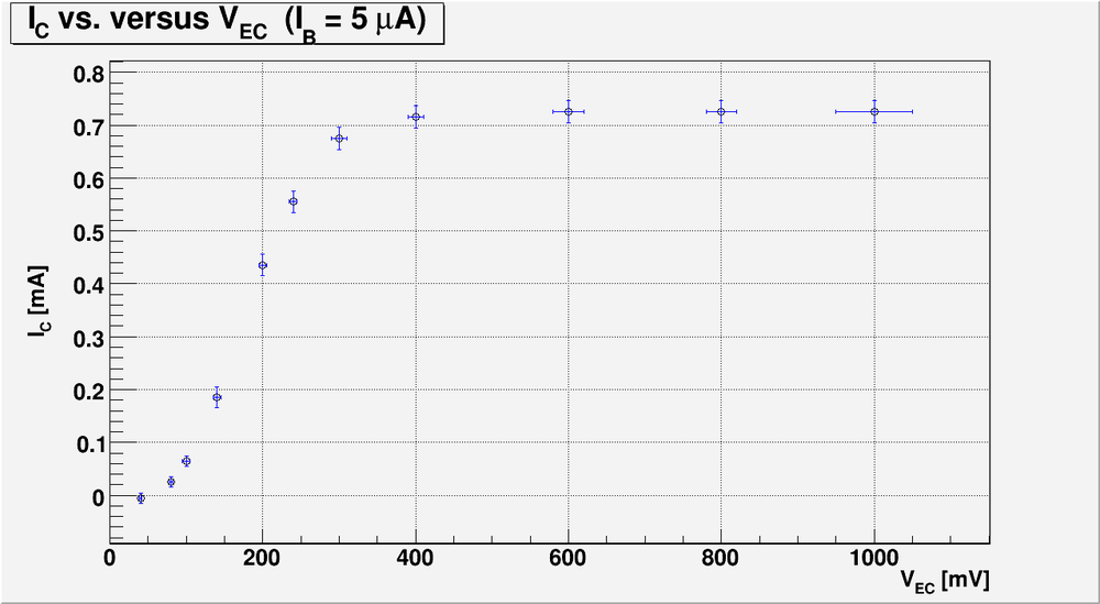
Bellow is my plot for the case of [math]I_B = 5 \mu A[/math]

Plot 5uA.png


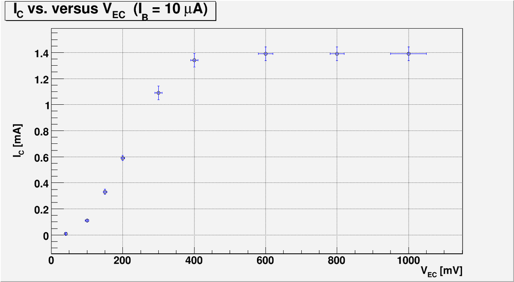
Bellow is my plot for the case of [math]I_B = 10 \mu A[/math]

Plot 10uA.png


6.) Overlay points from the transistor's data sheet on the graph in part 5.).(10 pnts)

I can not really do it because there are not good points to compare from data sheet. I can take for example this data from data sheet:

Table sheet 01.png

And from the table above I can only extract the range of [math]I_B[/math] like

1) [math]I_C = 0.1\ mA,\ V_{CE} = 1.0\ V \rightarrow I_B = \frac{I_C}{\beta} = \frac{0.1}{40..300} = (2.5 - 0.33)\ \mu A[/math]
2) [math]I_C = 1.0\ mA,\ V_{CE} = 1.0\ V \rightarrow I_B = \frac{I_C}{\beta} = \frac{0.1}{70..300} = (14.2 - 3.3)\ \mu A[/math]

And my measurements looks like:

1) [math]I_B = 2\ \mu A,\ I_C = 0.3\ mA,\ V_{CE} = 1.0\ V \rightarrow \beta = \frac{I_C}{I_B} = \frac{0.3\ mA}{2\ uA} = 150[/math]
2) [math]I_B = 5\ \mu A,\ I_C = 0.72\ mA,\ V_{CE} = 1.0\ V \rightarrow \beta = \frac{I_C}{I_B} = \frac{0.72\ mA}{5\ uA} = 144[/math]
3) [math]I_B = 10\ \mu A,\ I_C = 1.40\ mA,\ V_{CE} = 1.0\ V \rightarrow \beta = \frac{I_C}{I_B} = \frac{1.40\ mA}{10\ uA} = 140[/math]

First point to note that [math]I_C[/math] from my measurements and from data sheet are different so I can not really overlay them and compare. Second, I have specific values of [math]I_B[/math], otherwise from data sheet I have the range of [math]I_B[/math]. And third, I can't really plot this range of [math]I_B[/math] from data sheet on my plots just because my plot doesn't have the [math]I_B[/math] axis.


All I can do here is to say that my measured [math]\beta[/math] are inside the range of data sheet [math]\beta[/math].

Questions

1) Compare your measured value of [math]h_{FE}[/math] or [math]\beta[/math] for the transistor to the spec sheet? (10 pnts)


I will calculate my [math]\beta[/math] from my measurements above in active region like:

1)[math]I_B = 2\ \mu A[/math]:  [math]\beta = \frac{I_C}{I_B} = \frac{(0.298 \pm 0.010) mA}{(1.967 \pm 0.108) uA} = (151 \pm 9) [/math] 
2)[math]I_B = 5\ \mu A[/math]:  [math]\beta = \frac{I_C}{I_B} = \frac{(0.725 \pm 0.021) mA}{(4.862 \pm 0.121) uA} = (149 \pm 6) [/math] 
3)[math]I_B = 10\ \mu A[/math]:  [math]\beta = \frac{I_C}{I_B} = \frac{(1.391 \pm 0.052) mA}{(9.200 \pm 0.372) uA} = (151 \pm 8) [/math] 


And above values of [math]\beta[/math] are in agreement with range of [math]\beta[/math] from the spec sheet which is from 30 to 300. But I can not say nothing more because 1) my [math]I_C[/math] current doesn't correspond to published in data sheet. 2) My [math]\beta[/math] calculation is for specific value of [math]I_B[/math] current. But in the data sheet the range of [math]\beta[/math] is reported for specific values of [math]I_C[/math] and [math]V_{CE}[/math].


2) What is [math]\alpha[/math] for the transistor? [math]\alpha = \frac {I_{C}}{I_{E}}[/math] (10 pnts)

3) The base must always be more positive (negative) than the emitter for a npn (pnp) transistor to conduct I_C.(10 pnts)

4) For a transistor to conduct [math]I_{C}[/math] the base-emitter junction must be forward biased.(10 pnts)

5) For a transistor to conduct [math]I_{C}[/math] the collector-base junction must be reversed biased.(10 pnts)

Extra credit

Measure the Base-Emitter breakdown voltage. (10 pnts)


I expect to see a graph [math](I_{B} -vs- V_{BE} )[/math] and a linear fit which is similar to the forward biased diode curves. Compare your result to what is reported in the data sheet.


I used:

[math]R_B = (199.5 \pm 1.0)\ k\Omega [/math]
[math]R_E = (100.0 \pm 1.0)\ \Omega [/math]
[math]V_{CC} = (840 \pm 20)\ mV [/math]


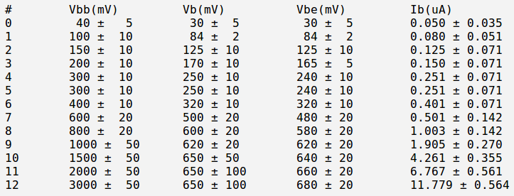
Below is the table with my measurements and current calculations:

Here I have used exact formula to calculate [math]I_B[/math]:

[math]I_{B} = \frac{V_{BB}-V_B}{R_B}[/math]

Table extra.png


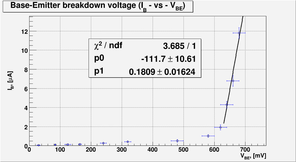
And bellow is my plot for the Base-Emitter breakdown voltage

Plot extra fitted.png


The fitting line is [math]I_B\ (\mu A) = (111.7 \pm 10.61) + (0.1809 \pm 0.01634)\ (mV) [/math]. The intersection this line with x-axis gives the forward turn on voltage:

[math]V_{BE} = \frac{p_0}{p_1} = \frac{111.7 \pm 10.61}{0.1809 \pm 0.01634} = (617.46 \pm 80.93)\ mV[/math]

Actually what we are measuring here is better to call the forward turn on voltage for base-emitter junction (Base-Emitter breakdown voltage is for reverse current measurement). From the data sheet this point (called the base-emitter saturation voltage) is 0.65 V and this point is inside my predicted values [math](617.46 \pm 80.93)\ mV[/math]


Go Back to All Lab Reports Forest_Electronic_Instrumentation_and_Measurement