TF EIM Chapt5
Bipolar Transistor
The Bipolar transistor concept
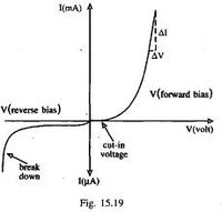
From the last chapter we saw a p-n junction diode which had similar characteristic current-vs- voltage responses when biased either in the forward direction or backward.
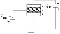
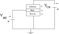
The bottom p-n junction, when forward biased, provides a large current with a small voltage bias.
The top half of the p-n-p transistor is reversed biased, providing a "throttle" for the large current from the lower half.
The electric field points to the "collector" in the depletion region enlarged by the reverse bias. This moves the majority charge carriers away from the collector-base junction. Once outside the depletion zone, the charge carriers rely on diffusion to escape the material.
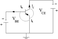
Bipolar transistor currents
- Conservation of Current
Here it is the case that the positive current is actually representing the flow of positively charged holes (in non-semi-conductors the current represent the opposite direction of the flowing electrons)
You might think that the base current is larger than the collector current because of the reverse bias on the collector which leads to the base having lower resistance than the collector.
The above is not the case.
The potential continuously draws electrons out of the emitter thus creating holes in the emitter. These holes diffuse into the base and are in a free-field region until they reach the depletion region between the collector and base.
While in the free-field region of the base they can do one of three things
- diffuse to the depletion region where they see the electric field and get swept into the collector.
- recombine with the mobile electrons in the base (the base is n-type material so electrons are the majority charge carriers)
- re-combine with electrons injected by into the base through the resistor
Usually the last two processes are more likely.
BUT if you make the emitter thin enough (less than the mean free path of the holes) then you can have the first process dominate such that most of the holes get swept into the collector before they get a chance to recombine.
As a result a large fraction of the current into the emitter () goes into the collector. ()
returning to conservation of current
So small changes in produce large changes in (You can control a large current using a small current )
- This is an amplifier!
- If you inject a signal into the base then the small changes in the base current will result in large changes in the collector current.
Transistor Physical features
As described above, the p-n-p junction is formed by "sandwiching" a thin n-type semicondor with 2 p-type semi-conductors.
The term "sandwiching" is in quotes because you DON'T glue 3 semiconductors together.
vertical diffuse planar transistor
Instead you start with a pure crystal of silicon that has been doped to to form the type os semi-conductor you wish to have as the COLLECTOR.
For now let's assume p-type, this means you dope pure silicon with boron. The collector is big (thick) because it has a lot of heat to dissipate.
Then you dope the crystal with impurities (Phosphorus) such that a thin n-type layer is formed, by diffusion, in the middle of the p-type crystal.
You then need to treat the top layer with dopant again to overcoming the n-type characteristics which are left over from forming the n-type base in the middle of the device AND create more holes with larger dopant than the collector. This step will directly influence the gain( and ) of the transistor.
The critical feature of the process is to establish abrupt changes in the doping which create sharp boundaries.
You then coat the collector side with a conductor like metallic aluminum.
On the side used to transport dopant you need to construct contacts for the base and emitter. To do this you need an insulation layer and a conductor layer which passes through the insulation and makes contact with the base and emitter material. You use a stencil to deposit an insulating layer of SiO2 which will have holes that leave the base and emitter semiconductor material exposed. Then you deposit metallic aluminum conductor into the holes.
The three layers
A transistor has three semi-conductor payers. The three layers occur in the order of
p-n-p= holes-electron-hole
n-p-n= electron-hole-electron
The three layers are formed from a single crystal such that the doping of the single crystal defines the boundaries. The three layers are not "glued" together.
Base-Emmiter-Collector
Testing for pnp or npn
You can use an Ohmmeter to tell if a transistor is pnp or npn.
Generally the base is the middle of the three pins for a bi-polar transistor.
If you put the voltmeters positive probe on the emitter lead and the ground probe onto the base lead, then a pnp transistor will yield a low resistance (1- 10 s).
If it is a npn transistor then the positive probe on the base and the ground on the emitter will yield the small resistance.
So it you know which leads are emitter and base you can determine transistor type.
If you know transistor type, you can determine which lead is the emitter.
You can test if the transistor is good or not using the table below with the Ohmeter set on the 1 range.
| type | ||||||
| pnp | high | low | high | low | high | high |
| npn | low | high | low | high | high | high |


