TF EIM Chapt5
Bipolar Transistor
The Bipolar transistor concept
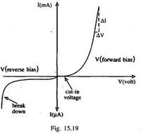
From the last chapter we saw a p-n junction diode which had similar characteristic current-vs- voltage responses when biased either in the forward direction or backward.
Transistor Physical features
The three layers
A transistor has three semi-conductor payers. The three layers occur in the order of
p-n-p= holes-electron-hole
n-p-n= electron-hole-electron
The three layers are formed from a single crystal such that the doping of the single crystal defines the boundaries. The three layers are not "glued" together.


