TF EIMLab13 Writeup
DC Bipolar Transistor Curves
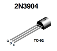
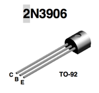
Data sheet for transistors.
Media:2N3904.pdfMedia:2N3906.pdf
Using 2N3904 is more straight forward in this lab.
Transistor circuit
1.) Identify the type (n-p-n or p-n-p) of transistor you are using and fill in the following specifications.
| Value | Description |
| 40 V | Collector-Base breakdown voltage |
| 6 V | Emitter-Base Breakdown Voltage |
| 40 | Maximum Collector Voltage |
| 200 mA | Maximum Collector Current |
| 625 mW | Transistor Power rating() |
| 30 - 300 | DC current gain |
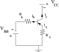
2.) Construct the circuit below according to the type of transistor you have.
Let .
variable power supply
.
I_B = 2 A = 1V/500 k
- = 5 A = 1V/200 k
- = 10 = 1V/100 k
3.) Measure the emitter current for several values of by changing such that the base current A is constant.
| V | A | V | mV | mA |
| 1.007 | 2 | 0.0704 | 1.2 | |
| 1.05 | 2 | 0.110 | 4.9 | |
| 1.02 | 2 | 0.133 | 8.9 | |
| 1.002 | 2 | 0.162 | 15.7 | |
| 1.002 | 2 | 0.184 | 21.1 | |
| 1.026 | 2 | 0.2287 | 32.3 | |
| 1.012 | 2 | 0.3157 | 39.5 | |
| 1.008 | 2 | 0.484 | 40.0 | |
| 1.008 | 2 | 1.023 | 40.3 | |
| 1.008 | 2 | 2.167 | 40.7 | |
| 1.008 | 2 | 2.960 | 40.8 | |
| 1.008 | 2 | 5.00 | 41.2 | |
4.) Repeat the previous measurements for A. Remember to keep so the transistor doesn't burn out
| V | A | V | mV | mA |
| 1.044 | 5 | 0.094 | 7 | |
| 1.053 | 5 | 0.134 | 19 | |
| 1.026 | 5 | 0.167 | 32 | |
| 1.003 | 5 | 0.200 | 47 | |
| 1.003 | 5 | 0.234 | 62 | |
| 1.02 | 5 | 0.269 | 77 | |
| 1.0 | 5 | 0.289 | 83 | |
| 1.07 | 5 | 0.442 | 101 | |
| 1.02 | 5 | 0.721 | 99 | |
| 1.02 | 5 | 1.04 | 100 | |
| 1.02 | 5 | 1.94 | 100 | |
| 1.02 | 5 | 2.96 | 101 | |
| 1.02 | 5 | 3.72 | 102 |
| V | A | V | mV | mA |
| 0.942 | 10 | 0.227 | 78.1 | |
| 1.005 | 10 | 0.245 | 94 | |
| 0.995 | 10 | 0.267 | 108 | |
| 1.068 | 10 | 0.31 | 138 | |
| 1.005 | 10 | 0.355 | 160 | |
| 0.996 | 10 | 1.032 | 197 | |
| 1.002 | 10 | 0.688 | 197 | |
| 0.996 | 10 | 2.175 | 199 | |
| 0.994 | 10 | 3.283 | 200 | |
| 0.992 | 10 | 4.66 | 202 |
5.) Graph -vs- for each value of and above. (40 pnts)
6.) Overlay points from the transistor's data sheet on the graph in part 5.).(10 pnts)
Questions
- Compare your measured value of or for the transistor to the spec sheet? (10 pnts)
- What is for the transistor?(10 pnts)
- The base must always be more _________(________) than the emitter for a npn (pnp)transistor to conduct I_C.(10 pnts)
- For a transistor to conduct I_C the base-emitter junction must be ___________ biased.(10 pnts)
- For a transistor to conduct I_C the collector-base junction must be ___________ biased.(10 pnts)


