Difference between revisions of "A W CAA apparatus"
(→HpGe) |
(→NaI) |
||
| Line 29: | Line 29: | ||
| − | The second detector employed in our coincidence set-up was a Sodium Iodide (NaI) detector. NaI detectors are a type of scintillation detector | + | The second detector employed in our coincidence set-up was a Sodium Iodide (NaI) detector. NaI detectors are a type of scintillation detector usually coupled to a photomultiplier tube (PMT). The NaI scintillator material is doped with thallium and fluoresces when excited by ionizing radiation. The thallium is used to increase the probability for photon emission. The emitted light strikes a photocathode, releasing at most one photoelectron per photon. The ejected electron is accelerated towards a system dynodes by an electric field. Additional electrons are knocked off each stage of the dynode as a result of the applied electric field resulting in a measurable signal that is collected at the anode and coupled to a coaxial BNC output connector. We used a Bicron model 3M3/3 detector with a <math>3 \times 3</math> inch crystal. The PMT voltage was set at -1000 V. A picture of the detector and its diagram can be seen on figures XX.YY and XX.YY. |
Revision as of 20:14, 17 October 2014
Detectors
HpGe
Type (npn or pnp): Ortec
Model #: SGD-GEM-50180P-S
Crystal dimensions: active diameter 65 mm (6.5 cm)
Operating voltage: 4600 V
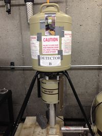
A high-purity germanium (HpGe) detector is the first of two detectors used in for our coincidence set-up. These detectors employ a germanium semiconductor to measure the energy of impinging radiation. In semiconductor detectors, the incident photon's energy is measured by the number of charge carriers set free in the material's valence band and transferred to the conduction band. An equal number of electronic vacancies or "holes" are created in the valance band. Placing the material between two electrodes and applying an electric field will give a measurable pulse. In order to reduce thermal excitations of valence electrons, the detector is cooled to liquid nitrogen temperatures. HpGe detectors have an energy resolution of 1 keV. We used a p-type germanium from Ortec model SGD-GEM-50180P-S with an active crystal diameter of 65 mm. The 4600 V detector bias was controlled by the SMART-INTERFACE computer software. FigureXX.YY shows the detector with a dewar attached that kept the detector cool for at least one week before additional nitrogen was required.
NaI
Type: Bicron
Model #: 3M3/3
Crystal dimensions: inches ( cm)
Operating voltage: -1000 V
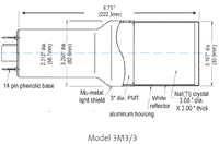
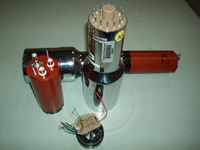
The second detector employed in our coincidence set-up was a Sodium Iodide (NaI) detector. NaI detectors are a type of scintillation detector usually coupled to a photomultiplier tube (PMT). The NaI scintillator material is doped with thallium and fluoresces when excited by ionizing radiation. The thallium is used to increase the probability for photon emission. The emitted light strikes a photocathode, releasing at most one photoelectron per photon. The ejected electron is accelerated towards a system dynodes by an electric field. Additional electrons are knocked off each stage of the dynode as a result of the applied electric field resulting in a measurable signal that is collected at the anode and coupled to a coaxial BNC output connector. We used a Bicron model 3M3/3 detector with a inch crystal. The PMT voltage was set at -1000 V. A picture of the detector and its diagram can be seen on figures XX.YY and XX.YY.
Geometry
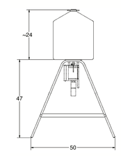
Samples were positioned on top of polyethylene blocks. Polyethylene replaced cement blocks to reduce the background from the cement blocks. The HpGe detector was suspended from a dewar 9.5 cm above the sample. The NaI detector is perpendicular to the HpGe detector and 6.7 cm from the sample. The NaI detector was shielded using two standard (2x4x8 inch) Pb bricks. A drawing of the apparatus is shown in Figure XX.YY.
Signal Processing
Analog output
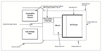
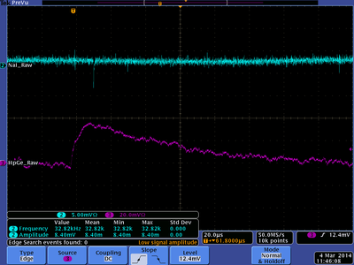
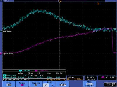
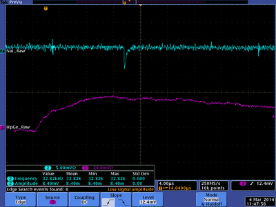
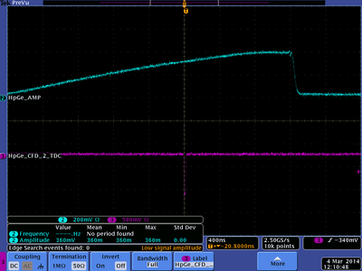
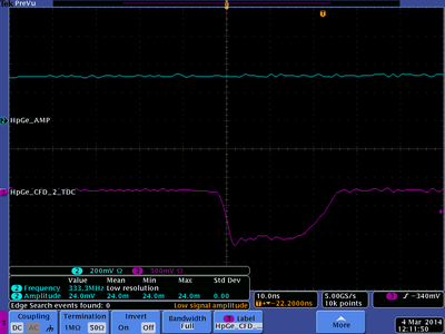
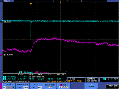
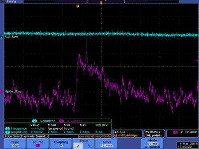
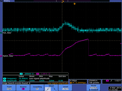
As seen in the HpGe detector diagram above, the electronic signal goes directly to a preamplifier, which converts the charge pulse from the detector to a voltage pulse or analog signal. This positive voltage signal has a short rise time and a very long decay time, with an amplitude of 20 mV as shown in figureXX.YY. The signal is next sent to an amplifier that provides a voltage gain to bring the pulse amplitude to 500 mV where it can more conveniently be processed. The signal shape has also changed, and now has a long rise time with a short decay, as seen in figureXX.YY.
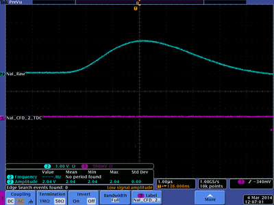
The NaI detector pre-amplified output analog signal comes from the the PMT and can also be seen in figureXX.YY. In contrast to the HpGe signal, the negative voltage NaI signal has a very narrow pulse width and a small amplitude of 5 mV. Sending the signal through the amplifier will invert the signal to a positive amplitude and broaden the pulse with a gradually rounded maximum peak amplitude of 200 mV.The signal is also more symmetric. The amplified signal can be seen alongside the HpGe amplified signal in figureXX.YY.
Analog amplification
Discrimination
Signal Trigger logic
Insert you paragraphs describing the apparatus
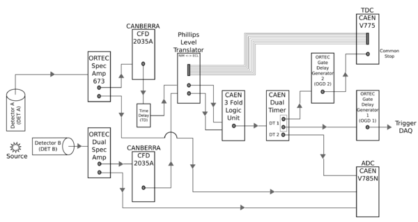
The coincidence counting set-up and modules path are as follows. A source is set atop a base constructed of hydrogen dense blocks. These were chosen to reduce the number of background energy spikes detected. The source is placed an equal distance from decorator A and detector B.
Detector A is positioned directly above the source. A high-purity germanium detector is being utilized for this set-up. The one outgoing signal enters a ORTEC 673 Spectroscopy Amplifier and the outgoing signal then passes through a CANBERRA CFD 2035A. The signal can then enter an optional CAEN CFD to produce a time delay, or can pass directly into a channel (1) of the Level Translator. The second outgoing signal from the Spec Amp goes to a peak sensing CAEN V785N. The output from this module goes to the DAQ.
Perpendicular from detector A and placed an equal distance from the source is detector B. This detector can either be a NaI-3 or a germanium detector depending on the source being counted. Detector B’s signal goes to a Post Amplifier and one outgoing signal goes to the above mentioned CAEN V785N and also to the DAQ. The second signal enters a CANBERRA CFD 2035A. The outgoing signal goes to a different channel (4) of the same Level Translator. A ribbon cable on the Level Translator module goes to a Time-to-Digital Converter (TDC) CAEN V775 that is operating in common start mode.
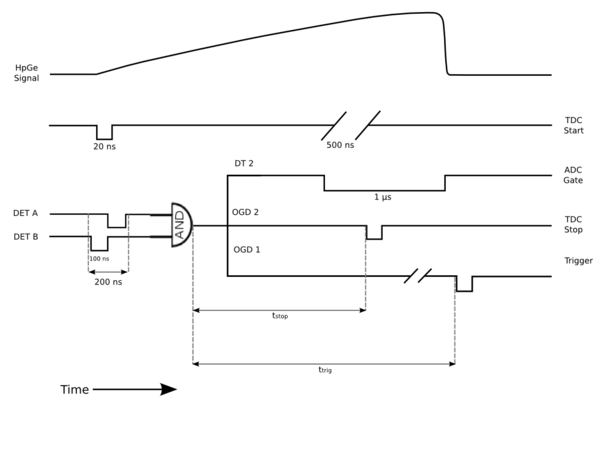
Both channels (1 and 4) of the Level Translator outgoing signal pass to a 3-fold Logic Unit which is used in both OR mode and AND mode to see coincidence lines. This data is collected in the Trig DAQ.
