Difference between revisions of "Sadiq Thesis Latex"
| Line 962: | Line 962: | ||
1.7 Photon spectrum of 12 MeV mono energy 10 million electrons impinge on a 1.016 mm thick tungsten target. . . . . . . . . . . 8 | 1.7 Photon spectrum of 12 MeV mono energy 10 million electrons impinge on a 1.016 mm thick tungsten target. . . . . . . . . . . 8 | ||
| − | [[ | + | [[image:hrrl_2011_mar_emit_test_quad_scan_quad.png | 300 px]] |
1.8 Apparatus used to measure the beam emittance. . . . . . . . . . . . . . . . . 11 | 1.8 Apparatus used to measure the beam emittance. . . . . . . . . . . . . . . . . 11 | ||
Revision as of 19:54, 9 July 2013
overlay positron energy distribution at T1 with what is seen at T2 for several values of Q7
Put the e+ simulated results results with experimentally detected results.
Flux weighted cross section for positron production.
Put the scintilator calibration in the thesis: Mean of ADC9 vs charge on the scope.
Separate simulated and experimental systematic errors, then put them together in conclusions.
Text
Introduction
\chapter{Introduction}
\section{Positron Beam}
Positrons are used in several disciplines of science such as chemistry, physics, material science, surface science, biology and nanoscience~\cite{Chemerisov:2009zz}. Different approaches are used to generate positrons. The main challenge is increasing the intensity (or current) of the positron beam. One of the most common methods used to generate a positron beam is an electron linear accelerator. The electron beam produces a positron beam via bremsstrahlung and pair production. One of the advantages of the linac based positrons is its variable energy and intensity. %Other applications of positron
Positron annihilation spectroscopy is a minimally invasive technique to detect defects in materials. It is based on the fact that positrons tend annihilate near defects in the material~\cite{Pos-app1}. A variable energy positron source may be used to probe for defects at different material depths.
\section{Positron Production Using Low Energy Linac}
%Low energy positron beam
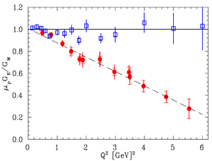
The nucleon electromagnetic form factors are fundamental quantities that related to the charge and magnetization distribution in the nucleon. Conventionally, the nucleon form factors are measured using Rosenbluth Technique (RT)~\cite{Rosenbluth1950}. The form factor scaling ratio, \begin{math}R=\mu _p G_{Ep} / G_{Mp}\end{math}, measured using this technique is around unity as shown in the figure below~\cite{PhysRevD.49.5671}. Since nighties, a technique using elastic electron-proton polarization transfer to measurement this ratio have been developed~\cite{PhysRevD.49.5671, PhysRevC.68.034325, WalkerThesis1989}. In this technique, form factor scaling ratio linearly decreases as the \begin{math}Q^2\end{math} increases, as shown in the Fig.~\ref{rosen-com-RPT}.
\begin{figure} \centering \includegraphics[scale=0.70]{1-Introduction/Figures/Sadiq_thesis_mot_RT_RPT_1.png} \caption{Form factor ratio, obtained by Rosenbluth Technique (hollow square) and results from Recoil Polarization Technique~\cite{PhysRevC.68.034325}.} \label{rosen-com-RPT} \end{figure}
The disagreement could arise from the fact the Rosenbluth Techqniue assumes that One Photon Exchange (OPE) during the scattering while the two–photon exchange (TPE), which depends weakly on \begin{math}Q^2\end{math}, could also become considerable with increasing \begin{math}Q^2\end{math}~\cite{PhysRevC.68.034325}. The contribution of TPE can be obtained by comparing the ratio of \begin{math}e^+~p\end{math} to \begin{math}e^-~p\end{math} ratio. The interference of OPE and TPE can also be studied in the process \begin{math}e^+e^- \rightarrow p\bar p\end{math}
\section{Positron Beam Generation from Bremsstrahlung}
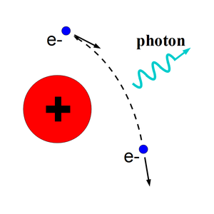
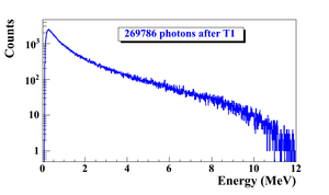
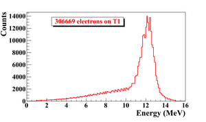
When a moving charged particle interacts with the electric field of another charged particle, it can be deflected and lose energy in the form of photons, as shown in Fig.~\ref{fig:Theo-Brem}. This interaction is known as the Bremsstrahlung process. The probability of this interaction increases with the atomic number of the material traversed by the incident charged particle. Fig.~\ref{fig:Brems_photon_Ene} shows the photon energy distribution when a 12 MeV electron distribution from Fig.~\ref{fig:Theo-Brems_ele_Ene} interacts with a 1 mm thick Tungsten target. The number of photons in this example produced decreases as the energy of the produced photon increases. The Bremsstrahlung photons are also likely to interact with the material.
\begin{figure} \centering \includegraphics[scale=0.40]{2-Theory/Figures/bremsstrahlung/brems.eps} \caption{Photon generation from Bremsstrahlung processes.} \label{fig:Theo-Brem} \end{figure}
The cross section of Bremsstrahlung process is give by Eq.~\ref{eq:Brem-cross}~\cite{brms-cors}
\begin{equation} d \sigma = 4 Z^2r_e^2 \alpha \frac{d \nu}{\nu} \left \{ \left (1 + \left( \frac{E}{E_0} \right )^2 \right ) \left [ \frac{\phi_1(\gamma)}{4} - \frac{1}{3} \ln Z -f(Z)\right ] - \frac{2E}{3E_0} \left [ \frac{\phi_2(\gamma)}{4} - \frac{1}{3} \ln Z -f(Z)\right ] \right \} \label{eq:Brem-cross} \end{equation}
where, $E_0$ is initial total energy of the electron, $E$ is final total energy of the electron, $\nu = \frac{E_0-E}{h}$ is energy of the emitted photon, and $Z$ is atomic number. $\gamma = \frac{100 m_ec^2 h \nu}{E_0 E Z^{1/3}}$ is charge screening parameter and $f(Z)$ is given by~\cite{tf-wiki}
\begin{equation} f(Z) = (Z \alpha)^2 \sum_1^{\infty} \frac{1}{ n [ n^2 + (Z \alpha)^2]} \end{equation}
where $\alpha = \frac{1}{137}$ is fine-structure constant, $\phi_1$ and $\phi_2$ are screening functions that depend on Z
\begin{figure} \centering \includegraphics[scale=0.50]{2-Theory/Figures/Brems_photon_Ene.png} \caption{Simulated Bremsstrahlung photon energy right after a tungsten foil.} \label{fig:Brems_photon_Ene} \end{figure}
\begin{figure} \centering \includegraphics[scale=0.50]{2-Theory/Figures/Brems_ele_Ene.png} \caption{Simulated electron energy distribution right before a tungsten foil.} \label{fig:Theo-Brems_ele_Ene} \end{figure}
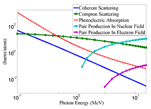
There are three competing processes that a photon can undergo when interacting with matter. At electron volt (eV) energies comparable to the electron atomic binding energy, the dominant photon interaction is via photoelectric effect. As the photon energy increases up to kilo-electron volt (keV) range, the Compton scattering process starts to be more dominant. Although the photon is totally absorbed during the photoelectric effect, photons merely lose energy when undergoing Compton scattering. As the photon energy reaches twice the rest mass energy of electron, 2 \begin{math} \times \end{math} 511~keV, pair production begins to happen. Pair production becomes dominant interaction process only for energies above 5 MeV~\cite{Krane}. In this process, a photon interacts with the electric field of the nucleus or the bound electrons and decays into an electron and positron pair.
\begin{figure} \centering \includegraphics[scale=0.4]{2-Theory/Figures/xcom/Xcom8.eps} \caption{Cross section of processes that photons interacts with tungsten~\cite{nistxcom}.} \label{fig:Theo-3pro-in-W} \end{figure}
Using natural unit \begin{math}c \equiv 1\end{math}, the differential cross-section for pair production can be expressed as~\cite{pair-cors, tf-wiki},
\begin{equation} \frac{d \sigma}{d \epsilon_1 d \theta_1 d \theta_2} = 8 \left ( \frac{\pi a}{\sinh (\pi a)} \right )^2 \frac{a^2}{2 \pi} \frac{e^2}{\hbar c} \left ( \frac{\hbar}{m_e c }\right )^2 \frac{\epsilon_1 \epsilon_2}{k^3} \theta_1 \theta_2 \end{equation}
\begin{description} \item[] \begin{math} \times \left \{ \frac{V^2(x)}{q^4} \left [ k^2 (u^2 + v^2) \xi \eta - 2 \epsilon_1 \epsilon_2 (u^2 \xi^2 + v^2 \eta^2 ) + 2 (\epsilon_1^2 + \epsilon_2^2)uv \xi \eta cos(\phi) \right ] \right . \end{math}
\end{description}
\begin{equation} \left . + a^2W^2(x) \xi^2 \eta^2 \left [ k^2(1 - (u^2+v^2)\xi \eta - 2 \epsilon_1 \epsilon_2 (u^2 \xi^2 + v^2 \eta^2) -2 (\epsilon_1^2 + \epsilon_2^2) u v \xi \eta \cos(\phi)\right ]\right \} \end{equation}
\noindent where $k$ is photon energy, $\theta_{1}$ and $\theta_2$ are the scattering angle of $e^+$ and $e^-$ respectively, $ \phi = \phi_1 - \phi_2$ is the angle between the $e^+$ and $e^-$ pair, $\epsilon_1$ and $\epsilon_2$ are the energy of the positron and electron respectively. Other constants are $u = \epsilon_1 \theta_1$, $v=\epsilon_2 \theta_2$, $\xi = \frac{1}{1+u^2}$, $\eta= \frac{1}{1+v^2}$, $q^2 = u^2 + v^2 + 2 u v \cos(\phi)$, $x= 1-q^2 \xi \eta$, $a = \frac{Ze^2}{\hbar c}$, and $V(x) = 1 + \frac{a^2}{(1!)^2} + \frac{a^2 (1+a^2) x^2}{(2!)^2} + \frac{a^2 (1+a^2)(2^2+a^2)x^4 x^2}{(3!)^2} + \cdots$, $W(x) = \frac{1}{a^2} \frac{d V(x)}{d x}$.
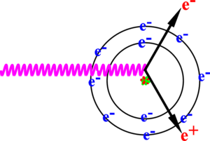
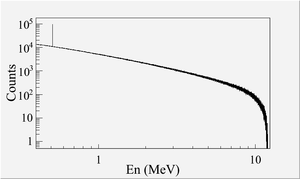
The positron and electron pairs are created back to back in the center of mass frame. In the lab frame, electrons and positrons are boosted forward, as demonstrated in the Fig.~\ref{fig:Theo-pair-pro}. The positron and electron carry away the energy from the photon that is in excess of 1.022~MeV. In the center of mass frame, the kinetic energy is equally shared. Photons with an energy above 1.022~MeV in the bremsstrahlung spectrum of Fig.~\ref{fig:Theo-brem} (a) have the potential to create electron and positron pairs. When the process of annihilation is included in the simulation, Fig.~\ref{fig:Theo-brem} (a) becomes Fig.~\ref{fig:Theo-brem} (b) showing a clear 511~keV peak on top of the bremsstrahlung spectrum. This 511 keV peak represents photon produced when the created positrons, from pair production, annihilates with an atomic electrons inside the tungsten target.
\begin{figure} \centering \includegraphics[scale=0.650]{2-Theory/Figures/Pair_Production/Pair_Production.png} \caption{Pair production.} \label{fig:Theo-pair-pro} \end{figure}
% Check the figures. \begin{figure} \begin{tabular}{cc} {\scalebox{0.9} [0.8]{\includegraphics{2-Theory/Figures/pair/on/Eng.eps}}} \\ (a) \\ {\scalebox{0.9} [0.8]{\includegraphics{2-Theory/Figures/pair/off/Eng.eps}}} \\ (b) \\ \end{tabular} \caption{Bremsstrahlung photon spectrum (a) and Bremsstrahlung spectrum after turning on pair production process (b).} \label{fig:Theo-brem} \end{figure}
Apparatus
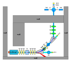
\chapter{Apparatus} \section{HRRL Beamline} The first step of this experiment is to deliver an electron beam with energy around 10~MeV and with sufficient current to the tungsten foil. A 16~MeV S-band High Repetition Rate Linac (HRRL) located at the Beam Lab of the Department of the Physics, Idaho State University is used to generate incident electron beam. The energy of the HRRL can be tunable between 3 to 16~MeV and its rep and its repetition rate is tunable between 1-300 Hz. Some basic parameters of the HRRL is given in the~\ref{tab:hrrl-par}. \begin{table} \centering \caption{Emittance Measurement Results.} \begin{tabular}{lcc} \toprule {Parameter} & {Unit} & {Value} \\ \midrule maximum energy & MeV & 16 \\ peak current & mA & 100 \\ repetition rate & Hz & 300 \\ absolute energy spread & MeV & 2-4 \\ macro pulse length & ns & $>$50 \\ \bottomrule \end{tabular} \label{tab:hrrl-par} \end{table} To construct a beamline can run on both positron and electron mode, the cavity is relocated to its current position and quadrupole and dipole magnets to transport the beam. As shown in Fig.~\ref{fig:app-hrrl-line} and described in Tab.~\ref{tab:app-hrrl-parts} more diagnostic tools like OTR/YAG screens, Faraday cups and toroids are installed to the new beamline for diagnostic purposes of electron beam. Energy slits are added to the beamline for the control of energy/momentum spread of the beam. A insertable tungsten foil target (T1) is placed between the 1st and 2nd triplets to produce positrons when the electron beam hits it. \begin{sidewaysfigure} \centering \includegraphics[scale=0.3]{3-Apparatus/Figures/HRRL_line.eps} \caption{HRRL beamline layout and parts.} \label{fig:app-hrrl-line} \end{sidewaysfigure}
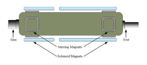
insert notation for steerer and solenioids inside cavity that are mentioned in section 2.2.2
Should S1 be labeled OTR?
There are 2 FCs labeled FC1
\begin{table} \centering \caption{HRRL Beamline Parts.} \begin{tabular}{ll} \toprule {Label} & {Beamline Element} \\ \midrule T1 & positron production target \\ T2 & positron annihilation target \\ Ens & energy slit \\ FC1, FC2 & Faraday cups \\ Q1,..., Q10 & quadrupoles \\ D1, D2 & dipoles \\ NaI & NaI detectors \\ OTR & optical transition radiation screen \\ YAG & yttrium aluminium garnet screen \\ \bottomrule \end{tabular} \label{tab:app-hrrl-parts} \end{table}
\section{Electron Beam Characterization}
\subsection{Emittance Measurement} Emittance is an important parameter in accelerator physics. If emittance with Twiss parameters are given at the exit of the gun, we will be able to calculate beam size and divergence any point after the exit of the gun. Knowing the beam size and beam divergence on the positron target will greatly help us study the process of creating positron. Emittance with twiss parameters are also key parameters for any accelerator simulations. Also, energy and energy spread of the beam will be measured in the emittance measurement.
\subsubsection{Emittance} In accelerator physics, Cartesian coordinate system was used to describe motion of the accelerated particles. Usually the z-axis of Cartesian coordinate system is set to be along the electron beam line as longitudinal beam direction. X-axis is set to be horizontal and perpendicular to the longitudinal direction, as one of the transverse beam direction. Y-axis is set to be vertical and perpendicular to the longitudinal direction, as another transverse beam direction. For the convenience of representation, we use z to represent our transverse coordinates, while discussing emittance. And we would like to express longitudinal beam direction with s. Our transverse beam profile changes along the beam line, it makes $z$ is function of $s$, $z(s)$. The angle of a accelerated charge regarding the designed orbit can be defined as $z'=\frac{dz}{ds}$.
If we plot z vs. z', we will get an ellipse. The area of the ellipse is an invariant, which is called Courant-Snyder invariant~\cite{Conte}. The transverse emittance $\epsilon$ of the beam is defined to be the area of the ellipse, which contains 90\% of the particles. Beam divergence and Twiss parameters related to the beam size and beam divergence by Eq.~\ref{eq:twiss-emit},
\begin{equation} \sigma_{x}(s)=\sqrt{\epsilon _x (s) \beta _x (s)},~ \sigma_{x'}(s)=\sqrt{\epsilon _x (s) \gamma _x (s)} . \label{eq:twiss-emit} \end{equation}
\subsubsection{Emittance Measurement}
The transition radiation first theoretically predicted by Ginzburg and Frank~\cite{Ginzburg-Frank} in 1946, that when a particle with charge passes the boundary of two medium emits radiation. The particle carries certain field when it passes through certain medium with certain motion~\cite{ENM-Jackson}. When it passes into the second medium, it has to reorganize its field characteristics at the boundary, and emit pieces of the field in the form electromagnetic radiation. The fields are emitted in the forward and backward directions~\cite{OTR-Gitter}. The backward radiated photons
An Optical Transition Radiation (OTR) based viewer was installed to allow measurements at the high electron currents available using the HRRL. The visible light from the OTR based viewer is produced when a relativistic electron beam crosses the boundary of two mediums with different dielectric constants. Visible radiation is emitted at an angle of 90${^\circ}$ with respect to the incident beam direction when the electron beam intersects the OTR target at a 45${^\circ}$ angle. These backward-emitted photons are observed using a digital camera and can be used to measure the shape and intensity of the electron beam based on the OTR distribution. The emittance measurement can be performed in a several ways~\cite{emit-ways, sole-scan-Kim}. The Quadrupole scanning method~\cite{quad-scan} was used to measure the emittance, Twiss parameters, and beam energy.
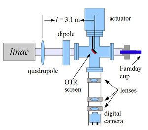
\subsubsection{Quadrupole Scanning Method} Fig.~\ref{q-scan-layout} illustrates the apparatus used to measure the emittance using the quadrupole scanning method. A quadrupole is positioned at the exit of the linac to focus or de-focus the beam as observed on a downstream view screen. The 3.1~m distance between the quadrupole and the screen was chosen in order to minimize chromatic effects and to satisfy the thin lens approximation. %The quadrupole and the screen are located far away to minimize chromatic effects and to increase the veracity of the thin lens approximation used to calculate beam optics. \begin{figure} \centering \includegraphics[scale=0.60]{3-Apparatus/MOPPR087f1.eps} \caption{Apparatus used to measure the beam emittance.} \label{q-scan-layout} \end{figure} Assuming the thin lens approximation, $\sqrt{k_1}L << 1$, is satisfied, the transfer matrix of a quadrupole magnet may be expressed as % thin lens approximation (sqrt{k1}*L << 1). In our case sqrt{k1}*L =0.07 \begin{equation} \label{quad-trans-matrix} \mathrm{\mathbf{Q}}=\Bigl(\begin{array}{cc} 1 & 0\\ -k_{1}L & 1 \end{array}\Bigr)=\Bigl(\begin{array}{cc} 1 & 0\\ -\frac{1}{f} & 1 \end{array}\Bigr), \end{equation} where $k_{1}$ is the quadrupole strength, $L$ is the length of quadrupole, and $f$ is the focal length. A matrix representing the drift space between the quadrupole and screen is given by \begin{equation} \label{drift-trans-matrix} \mathbf{\mathbf{S}}=\Bigl(\begin{array}{cc} 1 & l\\ 0 & 1 \end{array}\Bigr), \end{equation} where $l$ is the distance between the scanning quadrupole and the screen. The transfer matrix of the scanning region is given by the matrix product $\mathbf{SQ}$. In the horizontal plane, the beam matrix at the screen ($\mathbf{\sigma_{s}}$) is related to the beam matrix of the quadrupole ($\mathbf{\sigma_{q}}$) using the similarity transformation \begin{equation} \mathbf{\mathbf{\sigma_{s}=M\mathrm{\mathbf{\mathbf{\sigma_{q}}}}}M}^{\mathrm{T}}. \end{equation} where the $\mathbf{\sigma_{s}}$ and $\mathbf{\sigma_{q}}$ are defined as~\cite{SYLee} \begin{equation} \mathbf{\mathbf{\sigma_{s,\mathnormal{x}}=}}\Bigl(\begin{array}{cc} \sigma_{\textnormal{s},x}^{2} & \sigma_{\textnormal{s},xx'} \\ \sigma_{\textnormal{s},xx'} & \sigma_{\textnormal{s},x'}^{2} \end{array}\Bigr) ,\; \mathbf{\mathbf{\sigma_{q,\mathnormal{x}}}}=\Bigl(\begin{array}{cc} \sigma_{\textnormal{q},x}^{2} & \sigma_{\textnormal{q},xx'}\\ \sigma_{\textnormal{q},xx'} & \sigma_{\textnormal{q},x'}^{2} \end{array}\Bigr). \end{equation} \noindent %By defining the new parameters~\cite{quad-scan}, $A \equiv \sigma_{11},~B \equiv \frac{\sigma_{12}}{\sigma_{11}},~C \equiv\frac{\epsilon_{x}^{2}}{\sigma_{11}}$ By defining the new parameters~\cite{quad-scan} \begin{equation} A \equiv l^2\sigma_{\textnormal{q},x}^{2},~B \equiv \frac{1}{l} + \frac{\sigma_{\textnormal{q},xx'}}{\sigma_{\textnormal{q},x}^{2}},~C \equiv l^2\frac{\epsilon_{x}^{2}}{\sigma_{\textnormal{q},x}^{2}}, \end{equation} the matrix element $\sigma_{\textnormal{s},x}^{2}$, the square of the rms beam size at the screen, may be expressed as a parabolic function of the product of $k_1$ and $L$ \begin{equation} \sigma_{\textnormal{s},x}^{2}=A(k_{1}L)^{2}-2AB(k_{1}L)+(C+AB^{2}). \label{par_fit} \end{equation}
The emittance measurement was performed by changing the quadrupole current, which changes $k_{1}L$, and measuring the corresponding beam image on the view screen. The measured two-dimensional beam image was projected along the image's abscissa and ordinate axes. A Gaussian fitting function is used on each projection to determine the rms value, $\sigma_{\textnormal{s}}$ in Eq.~(\ref{par_fit}). Measurements of $\sigma_{\textnormal{s}}$ for several quadrupole currents ($k_{1}L$) is then fit using the parabolic function in Eq.~(\ref{par_fit}) to determine the constants $A$, $B$, and $C$. The emittance ($\epsilon$) and the Twiss parameters ($\alpha$ and $\beta$) can be found using Eq.~(\ref{emit-relation}). \begin{equation} \epsilon=\frac{\sqrt{AC}}{l^2},~\beta=\sqrt{\frac{A}{C}},~\alpha=\sqrt{\frac{A}{C}}(B+\frac{1}{l}). \label{emit-relation} \end{equation}
\subsection{The OTR Imaging System} The OTR target is 10 $\mu$m thick aluminum foil with a 1.25 inch diameter. The OTR is emitted in a cone shape with the maximum intensity at an angle of $1/\gamma$ with respect to the reflecting angle of the electron beam~\cite{OTR-Gitter}. Three lenses, 2 inches in diameter, are used for the imaging system to avoid optical distortion at lower electron energies. The focal lengths and position of the lenses are shown in Fig.~\ref{image_sys}. The camera used was a JAI CV-A10GE digital camera with a 767 by 576 pixel area. The camera images were taken by triggering the camera synchronously with the electron gun. \begin{figure} \centering {\scalebox{0.46} [0.46]{\includegraphics{3-Apparatus/MOPPR087f2.eps}}} {\scalebox{0.50} [0.50]{\includegraphics{3-Apparatus/MOPPR087f3}}} \caption{The OTR Imaging system.} \label{image_sys} \end{figure} \subsubsection{Quadrupole Scanning Experiment} The quadrupole current is changed to alter the strength and direction of the quadrupole magnetic field such that a measurable change in the beam shape is seen by the OTR system. Initially, the beam was steered by the quadrupole indicating that the beam was not entering along the quadrupole's central axis. Several magnetic elements upstream of this quadrupole were adjusted to align the incident electron beam with the quadrupole's central axis. First, the beam current observed by a Faraday cup located at the end of beam line was maximized using upstream steering coils within the linac nearest the gun. Second, the first solenoid nearest the linac gun was used to focus the electron beam on the OTR screen. Steering coils were adjusted to maximize the beam current to the Faraday cup and minimize the deflection of the beam by the solenoid first then by the quadrupole. A second solenoid and the last steering magnet, both near the exit of the linac, were used in the final step to optimize the beam spot size on the OTR target and maximize the Faraday cup current. A configuration was found that minimized the electron beam deflection when the quadrupole current was altered during the emittance measurements.
The emittance measurement was performed using an electron beam energy of 15~MeV and a 200~ns long, 40~mA, macro pulse peak current. The current in the first quadrupole after the exit of the linac was changed from $-$~5~A to 5~A with an increment of 0.2~A. Seven measurements were taken at each current step in order to determine the average beam width and the variance. Background measurements were taken by turning the linac's electron gun off while keep the RF on. Background image and beam images before and after background subtraction are shown in Fig.~\ref{bg}. A small dark current is visible in Fig.~\ref{bg}b that is known to be generated when electrons are pulled off the cavity wall and accelerated.
\begin{figure} \begin{tabular}{ccc} \centerline{\scalebox{0.42} [0.33]{\includegraphics{3-Apparatus/MOPPR087f4.eps}}} \\ (a)\\ \centerline{\scalebox{0.42} [0.33]{\includegraphics{3-Apparatus/MOPPR087f5.eps}}}\\ (b)\\ \centerline{\scalebox{0.42} [0.33]{\includegraphics{3-Apparatus/MOPPR087f6.eps}}}\\ (c) \end{tabular} \caption{Background subtracted to minimize impact of dark current; (a) a beam with the dark current and background noise, (b) a background image, (c) a beam image when dark background was subtracted.} \label{bg} \end{figure}
The electron beam energy was measured using a dipole magnet downstream of the quadrupole used for the emittance measurements. Prior to energizing the dipole, the electron micro-pulse bunch charge passing through the dipole was measured using a Faraday cup located approximately 50~cm downstream of the OTR screen. The dipole current was adjusted until a maximum beam current was observed on another Faraday cup located just after the 45 degree exit port of the dipole. A magnetic field map of the dipole suggests that the electron beam energy was 15~$\pm$~1.6~MeV. Future emittance measurements are planned to cover the entire energy range of the linac.
\subsubsection{Data Analysis and Results} Images from the JAI camera were calibrated using the OTR target frame. An LED was used to illuminate the OTR aluminum frame that has a known inner diameter of 31.75~mm. Image processing software was used to inscribe a circle on the image to measure the circular OTR inner frame in units of pixels. The scaling factor can be obtained by dividing this length with the number of pixels observed. The result is a horizontal scaling factor of 0.04327~$\pm$~0.00016~mm/pixel and vertical scaling factor of 0.04204~$\pm$~0.00018~mm/pixel. Digital images from the JAI camera were extracted in a matrix format in order to take projections on both axes and perform a Gaussian fit. The observed image profiles were not well described by a single Gaussian distribution. The profiles may be described using a Lorentzian distribution, however, the rms of the Lorentzian function is not defined. The super Gaussian distribution seems to be the best option~\cite{sup-Gau}, because rms values may be directly extracted.
Fig.~\ref{fig:par-fit} shows the square of the rms ($\sigma^2_{\textnormal{s}}$) $vs$ $k_1L$ for $x$ (horizontal) and $y$ (vertical) beam projections along with the parabolic fits using Eq.~\ref{fig:par-fit}. The emittances and Twiss parameters from these fits are summarized in Table~\ref{tab:results}. \begin{figure} \begin{tabular}{cc} {\scalebox{0.42} [0.4]{\includegraphics{3-Apparatus/MOPPR087f7.eps}}} {\scalebox{0.42} [0.4]{\includegraphics{3-Apparatus/MOPPR087f8.eps}}} \end{tabular} \caption{Square of rms values and parabolic fittings.} \label{fig:par-fit} \end{figure}
\begin{table} \centering \caption{Emittance Measurement Results.} \begin{tabular}{lcc} \toprule {Parameter} & {Unit} & {Value} \\ \midrule projected emittance $\epsilon_x$ & $\mu$m & $0.37 \pm 0.02$ \\ projected emittance $\epsilon_y$ & $\mu$m & $0.30 \pm 0.04$ \\ % normalized \footnote{normalization procedure assumes appropriate beam chromaticity.} emittance $\epsilon_{n,x}$ & $\mu$m & $10.10 \pm 0.51$ \\ %normalized emittance $\epsilon_{n,y}$ & $\mu$m & $8.06 \pm 1.1$ \\ $\beta_x$-function & m & $1.40 \pm 0.06$ \\ $\beta_y$-function & m & $1.17 \pm 0.13$ \\ $\alpha_x$-function & rad & $0.97 \pm 0.06$ \\ $\alpha_y$-function & rad & $0.24 \pm 0.07$ \\ micro-pulse charge & pC & 11 \\ micro-pulse length & ps & 35 \\ energy of the beam $E$ & MeV & 15 $\pm$ 1.6 \\ relative energy spread $\Delta E/E$ & \% & 10.4 \\
\bottomrule \end{tabular} \label{tab:results} \end{table}
\subsection{Conclusions} A diagnostic tool was developed and used to measure the beam emittance of the High Rep Rate Linac at the Idaho Accelerator Center. The tool relied on measuring the images generated by the optical transition radiation of the electron beam on a polished thin aluminum target. The electron beam profile was not described well using a single Gaussian distribution but rather by a super Gaussian or Lorentzian distribution. The larger uncertainties observed for $\sigma^2_y$ are still under investigation. The projected emittance of the High Repetition Rate Linac, similar to medical linacs, at ISU was measured to be less than 0.4~$\mu$m as measured by the OTR based tool described above when accelerating electrons to an energy of 15~MeV. The normalized emittance may be obtained by multiplying the projected emittance by the average relativistic factor $\gamma$ and $\beta$ of the electron beam. We plan to perform similar measurements over the energy range of the linac in the near future.
\section{Energy Scan}
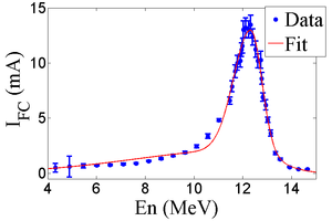
Energy scan was done to measure the energy profile of HRRL at nominal 12~MeV. A Faraday cup was placed at the end of the 45 degree beamline to measure the electron beam current bent by the first dipole. Dipole coil current were changed by 1~A increment and the Faraday cup currents were recorded. The relation between dipole current and beam energy is given in the appendix. A 12~MeV peak observed with long low energy tail. The energy distribution of HRRL can be described by two skewed Gaussian fits overlapping~\cite{sup-Gau}. The measurement result and fit are shown in Fig.~\ref{fig:En-Scan} and in Table~\ref{tab:En-Scan_resluts}
\begin{figure} \centering \includegraphics[scale=0.70]{3-Apparatus/HRRL-En-Scan_2_Assym_Gaussian_fit.png} \caption{HRRL energy scan (blue dots) and fit (red line) with two skewed Gaussian distribution.} \label{fig:En-Scan} \end{figure}
\begin{table} \centering \caption{Two Skewed Gaussian Parameters Describes Energy Distribution.} \begin{tabular}{lccc} \toprule {Parameter} & Unit & {First Gaussian} & {Second Gaussian} \\ \midrule amplitude A & & 2.14 & 10.88 \\ mean $\mu$ & MeV & 12.07 & 12.32 \\ sigma left $\sigma_L$ & MeV & 4.47 & 0.70 \\ sigma right $\sigma_R$ & MeV & 1.20 & 0.45 \\ \bottomrule \end{tabular} \label{tab:En-Scan_resluts} \end{table}
\section{Positron Detection}
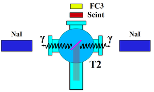
Positrons are transported to the end of the 90 degree beamline, experimental side of the room, which is located at the other side of the wall. A 6-way cross is placed at the end of the beamline to hold T2 and thin windows. 2 NaI detectors are used to detect photons generated during the annihilation process. The setup is shown in Fig.~\ref{fig:HRRL-pos-det-setup}. There are also a scintillator and a Faraday cup at the end of the beam tuning purposes. Most of the positrons reach T2 first thermalized inside and then annihilates. As they thermlize they lose their kinetic energy and photon energy emitted in annihilation is rest mess energy of electron, 511 keV. Two photons radiated back-to-back isotropically during the annihilation process. Two NaI detectors are in coincidence mode with short time window (tens of ns) to eliminate noises. Only when two photons happened to be in the incident in short time window, the signals are recorded as one entry.
\begin{figure} \centering \includegraphics[scale=0.50]{3-Apparatus/HRRL_Pos_detection.png} \caption{Positron Detection System. T2 (pink) is 45 degree placed with horizontal plane, then rotated towards left detector 45 degree.} \label{fig:HRRL-pos-det-setup} \end{figure}
\subsection{NaI Detectors}
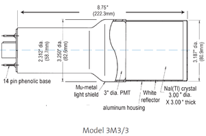
NaI crystals, shown as in Fig.~\ref{fig:PMT}, acquired from IAC were used to detect 511~keV photons from positron annihilation. Since the detectors had pulse length around 400~$\mu$s, the PMT bases were redesigned and rebuilt. The NaI detectors have two outputs, one is at second last dynode and one anode signal. PMT base configuration of the NaI detectors is shown in the Fig.~\ref{fig:PMT_base} and bases made shown in Fig.~\ref{fig:new_base_made}. It takes ADC 5.7~$\mu$s to convert analog signal to digital signal. The signal from anode was delayed 6~$\mu$s by long cable and sent to the ADC. PMT base take HV around -1150~V.
The PMT redesigned by changing few resistors and adding new capacitors bases because old base pulse length is around 400~$\mu$s. The new base pulse length is less than 1~$\mu$s. The NaI crystal is SAINT-GOBAIN CRYSTAL \& DETECTORS (MOD. 3M3/3) with sizes of 3”x3”. Bases were calibrated using Na-22 and Co-60 sources with photon peaks indicated in the Table~\ref{tab:Na22_Co60}.
\begin{table} \centering \caption{Radioactive sources and photon peaks.} \begin{tabular}{lccc} \toprule {Radioactive Sources} & Unit & First Peak & Second Peak \\ \midrule
Co-60                & keV   &  1173       &  1332       \\
Na-22                & keV   &  511        &  1275       \\
\bottomrule \end{tabular} \label{tab:Na22_Co60} \end{table}
\begin{figure} \centering \includegraphics[scale=0.6]{3-Apparatus/Modified_PMT.png} \caption{Modified PMT base design.} \label{fig:PMT_base} \end{figure}
\begin{figure} \centering \includegraphics[scale=0.4]{3-Apparatus/SAINT-GOBAIN_3M33.png} \caption{NaI crystal dimension.} \label{fig:PMT} \end{figure}
\begin{figure} \centering \includegraphics[scale=0.13]{3-Apparatus/IAC_NaI.png} \caption{NaI crystals and new bases.} \label{fig:new_base_made} \end{figure}
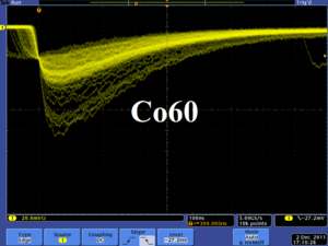
\begin{figure} \centering \includegraphics[scale=0.4]{3-Apparatus/NaI_Co60_Scope.png} \caption{Pulses from Co-60 source observed on the scope. The amplitude is about 60~mV. The rise time is larger than 50 ns, and the fall time is larger than 700~ns.} \label{fig:NaI_Co60_Scope} \end{figure}
\begin{figure} \centering \includegraphics[scale=0.75]{3-Apparatus/Figures/NaI_Calbration/NaI_Calb.eps} \caption{Calibrated NaI spectrum of Na-22 and Co-60 sources.} \label{fig:NaI-Calb} \end{figure}
fit the 511 peak in the above spectrum to show the energy resolution of a NaI detector
\subsection{Trigger for DAQ}
The trigger for DAQ required a coincidence between one or more NaI detectors and the electron accelerator gun pulse. The last dynode signals from left and right NaI detectors were inverted using a Ortec 474 amplifier and sent to a Constant Fraction Discriminator (CFD Model specs). RF noise from the accelerator is as large as the signal from the NaI detector. Since it is correlated in time with the gun pulse, the gun pulse was used to generate a VETO pulse that prevent the CFD from triggering on this RF noise. After this discrimination and RF noise rejection, the discriminated dynode signals were sent to an Octalgate Generator (Model) that increased the width of the logic signals to prevent multiple pulses during a single electron pulse. Then the signals were sent to Quad Coincidence to generate AND logic between electron gun and dynode signals. The logic is set as:
\begin{equation} (NaI~Left~\&\&~Gun~Trigger)~\&\&~(NaI~Rgiht~\&\&~Gun~Trigger). \end{equation}
This is to make sure we have trigger when photons back to back scatter to the NaI detectors when electron gun is on. Then this trigger was sent to ORTEC Gate \& Delay Generator. One of the out from gate generator was used to generate a gate to read analog signal from anode. Another output was delayed by 6~$\mu$s, necessary time to convert the analog signal from anode to digital signal, and used as trigger for the DAQ.
Simulation
\chapter{Simulation} A simulation was performed using the package G4beamline(ref Muons inc) to contrast its positron production efficiency prediction and investigate the impact of beam line elements on the efficiency. "G4beamline is a particle tracking and simulation program based on the Geant4 (reference G4) toolkit that is specifically designed to easily simulate beamlines and other systems using single-particle tracking." (insert reference for quote) Since the ratio of $e^{+}/e^{-}$ during the positron generation process is very low (on the order of 0.001) and the positron beam loss during the transportation is large, it was necessary to divide the simulation into 5 steps. A new electron beam event generator was created that reflected the electron beam properties of the HRRL shown in Figure 1.4. This event generator was used in the first simulation step to generate electrons according to a measurement made of the accelerator that was used in the experiment. Electrons are transported to Tungsten target (T1) in vacuum and produce positrons by first producing bremsstrahlung photons when will pair produce within the tungsten target. The second step is the transportation of the positrons generated at T1 to the entrance of first dipole magnet. The third step is the transportation of the positrons from the entrance of the first dipole magnet to the end of the second dipole. The fourth step is the transportation of the beam from the exit of the second dipole to the T2 target. The fifth step is the positron beam interaction with T2 and detection of the resulting 511~keV photons.
\section{Step 1 - The Electron Beam Generation and Transpiration to T1} In this step, an electron beam is generated to reflect the measured 12 GeV energy distribution shown in Fig.~\ref{fig:En-Scan} and the Twis parameters described in given in the Table~\ref{tab:En-Scan_resluts}. A series of virtual detectors are placed along the beamline to sample the beam. As an example, Fig.~\ref{fig:T1_UpD_DwD2} shows the three virtual detectors surrounding T1 that were used to record the momentum, energy and position of particles passing through those detectors. The electron beam is observed at DUPT1 (Detector 25.52~mm UPstream of T1) and positrons (or electrons and photons) generated during the interaction of electron beam with T1 are observed at DT1 (a detector that is parallel to the target) and DDNT1 (a detector 25.52~mm downstream of T1). %In the Fig.~\ref{fig:SimS1_pos_En_DDNT1}, $13.8 \times 10^{10}$ electrons shot at T1 and generated positrons positrons shown in blue.
\begin{figure} \centering \includegraphics[scale=0.50]{4-Simulation/Figures/sim_setup_T1_UpD_DwD2.png} \caption{T1 is positron production target with same geometry and material as real target. DUPT1 is virtual detector located upstream to sample incoming electron beam. DDNT1 is down stream virtual detector; DT1 is a virtual detector that is placed right after T1 with same angle as T1.} \label{fig:T1_UpD_DwD2} \end{figure}
\subsection{Positron Beam on DDNT1}
\begin{figure} \centering \includegraphics[scale=0.50]{4-Simulation/Figures/STSimS1_En_DDNT1_e+.png} \caption{Energy distribution of positrons detected on virtual detector DDNT1.} \label{fig:SimS1_pos_En_DDNT1} \end{figure}
overlay the energy distribution of electrons in DUPT1 and DDNT1 with the positrons in DDNT1 in the above picture
The first step of the simulation recorded the positrons, electrons, and photons that intersected virtual detector DDNT1 as a result of impinging 13,799,743,900 electrons onto target T1. Figure~\ref{fig:SimS1_pos_En_DDNT1} shows the energy distribution of the incident electrons before and after the 1 mm thick tungsten target (T1) as well as the energy distribution of positrons that escape from the back side of T1. The transverse spacial and angular distributions of positrons intersecting virtual detector DDNT1 are shown in Fig.~\ref{fig:SimS1_pos_En_DDNT1}.
\begin{figure} \begin{tabular}{cc} {\scalebox{0.3} [0.3]{\includegraphics{4-Simulation/Figures/STSimS1_X_DDNT1.png}}} & {\scalebox{0.3} [0.3]{\includegraphics{4-Simulation/Figures/STSimS1_Y_DDNT1.png}}} \\ (a) X DDNT1 & (b) Y DDNT1 \\ {\scalebox{0.3} [0.3]{\includegraphics{4-Simulation/Figures/STSimS1_XP_DDNT1.png}}} & {\scalebox{0.3} [0.3]{\includegraphics{4-Simulation/Figures/STSimS1_YP_DDNT1.png}}} \\ (c) X' DDNT1 & (d) Y' DDNT1\\ {\scalebox{0.42} [0.4]{\includegraphics{4-Simulation/Figures/STSimS1_XY_DDNT1.png}}} & {\scalebox{0.42} [0.4]{\includegraphics{4-Simulation/Figures/STSimS1_XY_DDNT1_zoom.png}}} \\ (e) X $vs.$ Y DDNT1 & (f) X $vs.$ Y DDNT1 zoom \\ \end{tabular} \caption{Transverse spacial and angular distribution of positrons on the virtual detector DDNT1.} \label{fig:DDNT1_results} \end{figure}
As can be seen on Fig~\ref{fig:DDNT1_results} (b) and (d), the y spacial distribution and y divergence distribution of the beam drop sharply on left side. Fig.~\ref{fig:DDNT1_results}~(f) illustrates that the depletion of events occurs in the region between -25.8 mm and -27.2 mm. Fig.~\ref{fig:sim-DDNT1-T1-geo} shows the geometry of the target T1 and the sensitive detector DDNT1. If the target size was increased, it would eventually intersected the detector DDNT1 at a distance of 25.8 mm from the beam center. The 1.4 mm wide stripe of low counts visible on DDNT1 appears to be a result of the target's thickness of 1.016 mm as projected onto the virtual detector at the 45$^{\circ}$ angle of intersection ($1.016\sqrt{2}=1.44$).
\begin{figure} \centering \includegraphics[scale=0.20]{4-Simulation/Figures/sim-DDNT1-T1-geo.png} \caption{Geometry of the target T1 and the virtual detector DDNT1.} \label{fig:sim-DDNT1-T1-geo} \end{figure}
As shown in Figs.~\ref{fig:DDNT1_YpY} (a) and (b), the positron angular divergence (Y') decreases as the location of positron emission from the target moves below the center of the beam line. Positrons are emitted from both the downstream and upstream side of the target. As shown in the figure ~\ref{fig:DDNT1_YpY}(b), positrons from the upstream side of the target do have a line of sight with and are able to intersect the virtual detector DDNT1 at angles below 45 degrees while positrons from the downstream side of the target begin to hit the detector at angles below 45 degrees. The 1.4 mm gap represents the transition of positrons between these two extremes.
\begin{figure} \begin{tabular}{cc} {\scalebox{0.3} [0.3]{\includegraphics{4-Simulation/Figures/STSimS1_YYP_DDNT1.png}}} & {\scalebox{0.3} [0.3]{\includegraphics{4-Simulation/Figures/STSimS1_YYP_DDNT1_zoom.png}}} \\ (a) Y' $vs.$ Y. & (b) Y' $vs.$ Y zoom. \\ \end{tabular} \caption{Positron beam distribution Y divergence vs. Y spacial distribution on DDNT1.} \label{fig:DDNT1_YpY} \end{figure}
Overlay a box representing the 1mm Tungsten target onto figure a above. Does figure (a) only show the generated positrons and not the generated positrons that make it to qquad q4?
\subsection{Positron Beam on DQ4 and DD1}
You need to describe the locations of virtual detectors DQ4 and DD1UP shown in figure 3.7
The positron beam energy distribution on virtual detector DQ4 placed at the entrance of Q4 and of D1 (DD1UP) are shown in Fig.~\ref{STSimS1_En_DQ4_DD1}. As it can be seen from the positron counts, nearly 90\% of them beam are lost during this process due to the large divergence of the positrons. \begin{figure} \begin{tabular}{ccc} \centerline{\scalebox{0.33} [0.33]{\includegraphics{4-Simulation/Figures/STSimS1_En_DQ4_e+.png}}} \\ (a) Positron energy distribution on DQ4 \\ \centerline{\scalebox{0.33} [0.33]{\includegraphics{4-Simulation/Figures/STSimS1_En_DD1_e+.png}}}\\ (b) Positron energy distribution on DD1 \\ \end{tabular} \caption{Positron beam energy distribution detected on the downstream of T2.} \label{STSimS1_En_DQ4_DD1} \end{figure}
\section{Step 2 - Transportation of the The Positron Beam after T1 to The Entrance of The First Dipole}
In this step, the positrons generated in the first step divided into 1~keV/c momentum bins and each bin is sampled individually since the momentum of the positrons related to their divergence. Multiple beams with individual weights generated at downstream T1 (at detector DDNT1) and transported to entrance of the D1 as shown in the Fig~\ref{fig:STSimSetupS2}. Virtual detectors are placed at the entrance of Q4 (DQ4) and of D1 (DD1UP) to track positrons. Beam detected at DD1UP is sampled for the generation of positron for the next step.
\begin{figure} \centering \includegraphics[scale=0.60]{4-Simulation/Figures/STSimSetupS2.png} \caption{Step 2 setup.} \label{fig:STSimSetupS2} \end{figure}
%\section{Comparing Positrons in Step 1 and Step 2} % %Positrons generated in step 1 and step 2 detected on the virtual detector located at the entrance of the first dipole is compared to validate the positrons generated in the step 2 is similar to the beam in step 1. Results, given in Fig.~\ref{fg:sim-s1s2-comp-en},~\ref{fg:sim-s1s2-comp-xy},~\ref{fg:sim-s1s2-comp-xpyp}, show that the beam regenerated in step 2 seems is similar to the one in step 1. % %\begin{figure} %\begin{tabular}{cc} %\centerline{\scalebox{0.6} [0.6]{\includegraphics{4-Simulation/Figures/s/s1/EnDD1.eps}}} \\ %(a) Beam Energy in step 1\\ % \\ %\centerline{\scalebox{0.6} [0.6]{\includegraphics{4-Simulation/Figures/s/s2/EnDD1.eps}}}\\ %(b) Beam Energy in step 2\\ %\end{tabular} %\caption{Comparison of positron energy in first and second steps at virtual detector located at the entrance of first dipole.} %\label{fg:sim-s1s2-comp-en} %\end{figure} % %\begin{sidewaysfigure} %\begin{tabular}{cc} %{\scalebox{0.5} [0.6]{\includegraphics{4-Simulation/Figures/s/s1/xDD1.eps}}} & {\scalebox{0.5} [0.6]{\includegraphics{4-Simulation/Figures/s/s2/xDD1.eps}}} \\ %(a) Beam X-projection in step 1 & (b) Beam X-projection in step 2 \\ %{\scalebox{0.5} [0.6]{\includegraphics{4-Simulation/Figures/s/s1/yDD1.eps}}} & {\scalebox{0.5} [0.6]{\includegraphics{4-Simulation/Figures/s/s2/yDD1.eps}}} \\ %(c) Beam Y-projection in step 1 & (d) Beam Y-projection in step 2 \\ %\end{tabular} %\caption{Comparison of positron transverse beam profile in first and second steps at virtual detector located at the entrance of first dipole.} %\label{fg:sim-s1s2-comp-xy} %\end{sidewaysfigure} % %\begin{sidewaysfigure} %\begin{tabular}{cc} %{\scalebox{0.5} [0.6]{\includegraphics{4-Simulation/Figures/s/s1/xPDD1.eps}}} & {\scalebox{0.5} [0.6]{\includegraphics{4-Simulation/Figures/s/s2/xPDD1.eps}}} \\ %(c) Beam divergence X-projection in step 1& (d) Beam divergence X-projection in step 2\\ %{\scalebox{0.5} [0.6]{\includegraphics{4-Simulation/Figures/s/s1/yPDD1.eps}}} & {\scalebox{0.5} [0.6]{\includegraphics{4-Simulation/Figures/s/s2/yPDD1.eps}}} \\ %(e) Beam divergence Y-projection in step 1 & (f) Beam divergence Y-projection in step 2 \\ %\end{tabular} %\caption{Comparison of positron transverse divergence in first and second steps at virtual detector located at the entrance of first dipole.} %\label{fg:sim-s1s2-comp-xpyp} %\end{sidewaysfigure}
\section{Step 3 - Generation of Positrons at the Entrance of the First Dipole and Their Transporting and Detection}
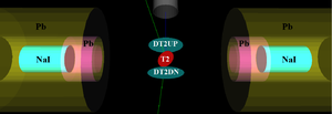
In this step, positrons are generated at the entrance of the first dipole (as shown DD1UP shown in Fig.~\ref{fig:STSimSetupS2}) by sampling the beam at the same location in previous step. Beam then transported down to T2 located at the end the beamline as shown in Fig.~\ref{fig:T2}. Two virtual detectors are placed to detected incoming positrons before and after T2. NaI virtual detectors are placed horizontally to detect photons. Pb shielding are placed around NaI detectors with openings facing T2. When a positron annihilate inside T2, two back to back scattered 511 keV photons are generated with same event number. NaI detectors count 1 event when they both detect 511 photons with same event number.
\begin{figure} \centering \includegraphics[scale=0.45]{4-Simulation/Figures/HRRL_T2.png} \caption{T2 and virtual detectors located upstream (DT2UP) and downstream (DT2DN) of T2. NaI dettectos and Pb shielding.} \label{fig:T2} \end{figure}
\subsection{Transport Efficiency}
%In this step, 14,359,380,000 positrons generated at DD1. By using the DQ4 and DDNT1 to DD1 ratios of we obtained from previous two steps, one can calculate that it is equivalent generating 57,559,974,511,209.3 at DDNT1, and detecting 375,891,831,521 at DQ4 and 14,359,380,000 at DD1 (i.e. DDNT1:57,559,974,511,209->DQ4:375,891,831,521->DD1:14,359,380,000). %Positrons are generated by $7.2528135 \times 10^{16}$ electrons incident on T1. $5.7559974511209 \times 10^{13}$ Positrons are generated by $7.253 \times 10^{16}$ electrons incident on T1 and $5.756 \times 10^{13}$ generated positrons. The transported positrons detected along the beamline. The beam lost is shown in Table~\ref{tab:app-hrrl-par} and Fig.~\ref{fig:TransEff}. Detector efficiency is taken into consideration with coincidence mode.
\begin{sidewaystable} \centering \caption{Transportation Efficiency} \begin{tabular}{lccccc} \toprule
 Energy         &  Generated at T1          &   Entered Q4              & Entered D1               &  Reaches T2            &  NaI Detectors \\
 (MeV)          &                           &                           &                          &                        &  in Coincidence   \\
\midrule $1.02 \pm 0.25$ & $2.52888 \times 10^{12} $ & $1.36481 \times 10^{10} $ & $1.36760 \times 10^{9} $ & $1.07070 \times 10^{4} $ & $6$\\ $1.50 \pm 0.25$ & $4.91629 \times 10^{12} $ & $2.74778 \times 10^{10} $ & $2.75965 \times 10^{9} $ & $1.40228 \times 10^{5} $ & $53 $\\ $2.15 \pm 0.25$ & $6.47248 \times 10^{12} $ & $3.75594 \times 10^{10} $ & $3.76997 \times 10^{9} $ & $9.58080 \times 10^{6} $ &$477 $\\ $2.50 \pm 0.25$ & $6.79791 \times 10^{12} $ & $4.05435 \times 10^{10} $ & $4.06923 \times 10^{9} $ & $1.19020 \times 10^{6} $ & $517 $\\ $3.00 \pm 0.25$ & $6.63138 \times 10^{12} $ & $4.06935 \times 10^{10} $ & $4.08565 \times 10^{9} $ & $1.19604 \times 10^{6} $ & $488 $\\ $3.50 \pm 0.25$ & $6.11215 \times 10^{12} $ & $3.88598 \times 10^{10} $ & $3.89856 \times 10^{9} $ & $1.19380 \times 10^{6} $ & $474 $\\ $4.02 \pm 0.25$ & $5.34016 \times 10^{12} $ & $3.50619 \times 10^{10} $ & $3.52110 \times 10^{9} $ & $1.15945 \times 10^{6} $ & $472 $\\ $4.50 \pm 0.25$ & $4.57640 \times 10^{12} $ & $3.09881 \times 10^{10} $ & $3.10839 \times 10^{9} $ & $1.09549 \times 10^{6} $ &$ 444 $\\ $5.00 \pm 0.25$ & $3.76900 \times 10^{12} $ & $2.65371 \times 10^{10} $ & $2.66784 \times 10^{9} $ & $1.01029 \times 10^{6} $ & $392 $\\ $5.50 \pm 0.25$ & $3.01205 \times 10^{12} $ & $2.20521 \times 10^{10} $ & $2.21408 \times 10^{9} $ & $9.06707 \times 10^{5} $ & $354 $\\
%$1.015 \pm 0.25$ & $2.52888e+012 \pm 1.59024e+006$ & $1.36481e+010 \pm 116825$ & $1.3676e+009 \pm 36981$ & $10707 \pm 103.475$ & $6.0112 pm 2.45177$\\ %$1.5 \pm 0.25$ & $4.91629e+012 \pm 2.21727e+006$ & $2.74778e+010 \pm 165764$ & $2.75965e+009 \pm 52532.4$ & $140228 \pm 374.47$ & $52.7136 pm 7.26041$\\ %$2.15 \pm 0.25$ & $6.47248e+012 \pm 2.54411e+006$ & $3.75594e+010 \pm 193803$ & $3.76997e+009 \pm 61400.1$ & $958080 \pm 978.816$ & $477.197 pm 21.8448$\\ %$2.5 \pm 0.25$ & $6.79791e+012 \pm 2.60728e+006$ & $4.05435e+010 \pm 201354$ & $4.06923e+009 \pm 63790.5$ & $1.1902e+006 \pm 1090.96$ & $516.963 pm 22.7368$\\ %$3 \pm 0.25$ & $6.63138e+012 \pm 2.57515e+006$ & $4.06935e+010 \pm 201726$ & $4.08565e+009 \pm 63919.1$ & $1.19604e+006 \pm 1093.64$ & $487.37 pm 22.0764$\\ %$3.5 \pm 0.25$ & $6.11215e+012 \pm 2.47228e+006$ & $3.88598e+010 \pm 197129$ & $3.89856e+009 \pm 62438.4$ & $1.1938e+006 \pm 1092.61$ & $473.96 pm 21.7706$\\ %$4.02 \pm 0.25$ & $5.34016e+012 \pm 2.31088e+006$ & $3.50619e+010 \pm 187248$ & $3.5211e+009 \pm 59338.9$ & $1.15945e+006 \pm 1076.78$ & $471.648 pm 21.7175$\\ %$4.5 \pm 0.25$ & $4.5764e+012 \pm 2.13925e+006$ & $3.09881e+010 \pm 176034$ & $3.10839e+009 \pm 55752.9$ & $1.09549e+006 \pm 1046.66$ & $444.366 pm 21.08$\\ %$5 \pm 0.25$ & $3.769e+012 \pm 1.94139e+006$ & $2.65371e+010 \pm 162902$ & $2.66784e+009 \pm 51651.2$ & $1.01029e+006 \pm 1005.13$ & $392.115 pm 19.8019$\\ %$5.5 \pm 0.25$ & $3.01205e+012 \pm 1.73553e+006$ & $2.20521e+010 \pm 148499$ & $2.21408e+009 \pm 47054$ & $906707 \pm 952.212$ & $353.736 pm 18.8079$\\
\bottomrule \end{tabular} \label{tab:app-hrrl-par} \end{sidewaystable}
\begin{figure} \centering \includegraphics[scale=0.70]{4-Simulation/Figures/Transporation_Efficiency/Ef.eps} \caption{Beam loss during transportation.} \label{fig:TransEff} \end{figure}
\subsection{Detector efficiency}
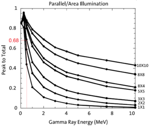
According to the detector efficiency chart, shown if Fig.~\ref{fig:NaI_Ef} obtained from SAINT-GOBIAN CRYSTALS~\cite{NaI-Eff}, at 511~keV, NaI crystals has 68\% efficiency. If they are in coincidence, their efficiency is 68\% * 68\% =46.24\%.
\begin{figure} \centering \includegraphics[scale=0.50]{4-Simulation/Figures/NaI_Ef_2.png} \caption{NaI detector efficiency~\cite{NaI-Eff}.} \label{fig:NaI_Ef} \end{figure}
\begin{figure} \centering \includegraphics[scale=0.60]{4-Simulation/Figures/overlay/e+_Generated_and_Detected.eps} \caption{Positrons generated detected on virtual detector DDNT1 and 511 keV counts detected by NaI detectors in coincidence mode (100 \% efficiency assumed).} \label{fig:e+_Generated_and_Detected} \end{figure}
%\begin{figure} %\centering %\includegraphics[scale=0.70]{4-Simulation/Figures/S2E/S2E.eps} %\caption{Results of simulation of positron generation and transportation process.} %\label{fig:S2E} %\end{figure} % % %\begin{sidewaysfigure} %\centering %\includegraphics[scale=1.2]{4-Simulation/Figures/S2E/S2E_32.eps} %\caption{Results of simulation of positron generation and transportation process.} %\label{fig:S2E_32} %\end{sidewaysfigure}
\section{Quadrupole Triplet Collection Efficiency Study}
Quadrupole triplet positron collection and transportation efficiency was studied by regenerating positrons after T1. Several quadrupole current settings were simulated shown in the Table.~\ref{tab:triplet-eff}. 5475869400 positrons generated and transported to the entrance of the D1, first dipole. A virtual detector is located at the entrance of the D1 to study collection and transportation efficiency of the triplet system. As it can be seen from the table, for different quadrupole settings, there are not any significant difference in number of positrons and their position and momentum distributions. On average, 3590413 positrons entered D1. The ratio of positrons generated to the ones enter D1 is 1525:1.
\begin{sidewaystable} \centering \caption{Quadrupole Triplet System Collection and Transportation Efficiency Data.} \begin{tabular}{cccccccccccccc} \toprule
Q4 & Q5 & Q6 & Entries & $x$ & $\sigma_{x} $ & y & $\sigma_{y}$ & $P_{x}$ & $\sigma_{P_{x}}$ & $P_{y}$ & $\sigma_{P_{y}}$ & $P_{z}$ & $\sigma_{P_{z}}$ \\
\midrule -1 & 2 & -1 & 3587220 & -0.004534 & 12 & 0.03058 & 12 & $3.0190 \times 10^{-5}$ & 0.04613 & -0.002159 & 0.04553 & 3.848 & 1.875 \\ -2 & 4 & -2 & 3591423 & -0.012230 & 12 & 0.04902 & 12 & $2.1870 \times 10^{-5}$ & 0.04612 & -0.002109 & 0.04554 & 3.848 & 1.875 \\ 1 & -2 & 1 & 3591509 & -0.009171 & 12 & 0.04015 & 12 & $-1.493 \times 10^{-5}$ & 0.04616 & -0.002154 & 0.04557 & 3.849 & 1.876 \\ 1 & 2 & 1 & 3589854 & -0.005396 & 12 & 0.03384 & 12 & $-1.779 \times 10^{-5}$ & 0.04615 & -0.002156 & 0.04556 & 3.849 & 1.876 \\ 2 & -4 & 2 & 3592977 & -0.007413 & 12 & 0.03225 & 12 & $-3.261 \times 10^{-6}$ & 0.04615 & -0.002173 & 0.04549 & 3.849 & 1.876 \\ 2 & 4 & 2 & 3589495 & -0.004142 & 12 & 0.03271 & 12 & $3.0420 \times 10^{-6}$ & 0.04616 & -0.002183 & 0.04554 & 3.849 & 1.875 \\ % & & & & & & & & & & & & & \\ \bottomrule \end{tabular} \label{tab:triplet-eff} \end{sidewaystable}
\section{Error Study}
Magnet settings are changed as shown Table.~\ref{tab:sim-error}. NaI detectors are in coincidence mode.
\begin{sidewaystable} \centering \caption{Systematic Error Study.} %\begin{tabular}{cccccccccccc} \begin{tabular}{llllllllllll} \toprule % $0.765-1.265$ & $1.25-1.75$& $1.85-2.35$ & $2.25-2.75$ & $2.75-3.25$ & $3.25-3.75$ & $3.77-4.27$ & $4.25-4.75$ & $4.75-5.25$ & $5.25-5.75$ \\ % MeV & MeV & MeV & MeV & MeV & MeV & MeV & MeV & MeV & MeV \\ D1 & Max & Min & Max & Min & Max & Max & Min & Min & Def &\\ Q7 & Def & Def & Def & Def & Max & Min & Min & Def & Def &\\ D2 & Max & Min & Def & Def & Def & Def & Def & Def & Def &\\ \midrule Energy & & & & & & & & & & Average \\ \midrule 0.77 - 1.27 MeV & 12 & 6 & 1 & 3 & 5 & 1 & 1 & 2 & 6 & $ 4 \pm 4$ \\ 1.25 - 1.75 MeV & 78 & 72 & 72 & 77 & 66 & 89 & 75 & 60 & 78 & $74 \pm 8$ \\ 1.85 - 2.35 MeV & 591 & 580 & 581 & 576 & 535 & 630 & 588 & 535 & 583 & $578 \pm 29$ \\ 2.25 - 2.75 MeV & 635 & 610 & 607 & 602 & 616 & 611 & 616 & 625 & 572 & $610 \pm 17$ \\ 2.75 - 3.25 MeV & 597 & 604 & 605 & 593 & 586 & 632 & 589 & 573 & 577 & $595 \pm 18$ \\ 3.25 - 3.75 MeV & 579 & 588 & 586 & 589 & 575 & 582 & 553 & 553 & 565 & $574 \pm 14$ \\ 3.77 - 4.27 MeV & 562 & 491 & 566 & 563 & 553 & 564 & 559 & 550 & 564 & $552 \pm 24$ \\ 4.25 - 4.75 MeV & 525 & 520 & 523 & 520 & 508 & 525 & 514 & 511 & 530 & $520 \pm 7$ \\ 4.75 - 5.25 MeV & 469 & 4774 & 482 & 464 & 455 & 474 & 451 & 466 & 464 & $467 \pm 10$ \\ 5.25 - 5.75 MeV & 432 & 423 & 427 & 405 & 418 & 422 & 429 & 418 & 419 & $421 \pm 8$ \\
\bottomrule \end{tabular} \label{tab:sim-error} \end{sidewaystable}
Experiment
\chapter{Experiment}
\section{Runs}
The annihilation target T2 is can be inserted or removed from the center of the beamline. This allow two kind runs, T2 in and T2 out. When T2 is in the positions are delivered to T2 and thermalize and annihilate produces 511 KeV photons. This photons are detected by the NaI detectors as shown in Fig.~\ref{fig:HRRL-En-Scan}. When T2 is out, positrons exits beamlien and transported to the beam dump. NaI detectors are shielded with Pb bricks from the beam dump. T2 out runs serve as background measurements.
\begin{figure} \centering \includegraphics[scale=0.50]{3-Apparatus/NaI_Setup.png} \caption{Positron detection using T2 and NaI detectors.} \label{fig:HRRL-En-Scan} \end{figure}
T2 is placed inside a 6-way cross and two horizontal side it sealed with thin windows. Two NaI detectors placed horizontally to T2, perpendicular to the 90 degree beamline and pointed to this windows. The spectrum taken with T2 in and out are shown in the Fig.~\ref{fig:in-out-runs}.
\begin{figure} \centering \begin{tabular}{cc}
{\scalebox{0.73} [0.70]{\includegraphics[scale=0.40]{3-Apparatus/r3737_sub_r3736_left.png}}} & {\scalebox{0.73} [0.70]{\includegraphics[scale=0.40]{3-Apparatus/r3737_sub_r3736_right.png}}} \\ (a) Original spectrum on left NaI. & (b) Original spectrum on right NaI.\\ & \\ & \\ {\scalebox{0.73} [0.70]{\includegraphics[scale=0.40]{3-Apparatus/r3737_sub_r3736_left_with_cut.png}}} & {\scalebox{0.73} [0.70]{\includegraphics[scale=0.40]{3-Apparatus/r3737_sub_r3736_right_with_cut.png}}} \\
(c) Spectrum with cut on left NaI. & (d) Spectrum with cut on right NaI.\\ & \\ \end{tabular} \caption{T2 in run (red) and T2 out background run (blue) time normalized spectrum. Top row shows original spectrum and bottom row shows incidents only happen in 511~keV peak coincidently on both detectors.} \label{fig:in-out-runs} \end{figure}
Run No. 3735 (T2 in) and run No. 3736 (T2 out) in the Fig.~\ref{fig:in-out-runs}, the two sub-figures acquired by cut that only incidents happened in 511~keV peak coincidently on both detectors. The positron counts extracted by subtracting background (blue in figure) and integrating the peak. The integral shown in red is from the background is subtracted spectrum. The run parameters of Run No. 3735 is given in Table.~\ref{tab:run3735}
\begin{table} \centering \caption{Run Parameters of Run No. 3735.} \begin{tabular}{lll} \toprule {Parameter} & {Unit} & {Value} \\ \midrule run number & & 3735 \\ repetition rate & Hz & 300 \\ run time & s & 1002 \\ pulses & & 301462 \\ events & & 9045 \\ e+ Counts NaI Detectors & & 256 $\pm$ 16\\ \bottomrule \end{tabular} \label{tab:run3735} \end{table}
\section{Electron Current Estimation}
A photon scintillator was placed between quadrupole 9 and quarupole 10 shown as in the Fig.~\ref{fig:Scint_e-} and used as electron beam monitor. To calibrate this scintillator electron beam changed incrementally and the charge was measured both on oscilloscope and ADC. As the electron beam increases the beam charge observed on the scope increased and the photon peak in the ADC also shifted towards right end of the spectrum. The measured results are shown in the Table~\ref{tab:scint_calb}. The result shows that the relation between electron beam current and scintillator ADC channel number is linear, $(0.93 \pm 0.14)/50$ nVs/(ADC channel number). The spectrum taken is shown in Fig~\ref{fig:ADC-CH9}.
\begin{figure} \centering \includegraphics[scale=0.10]{5-Experiment/Hrrl_pos_jul2012_setup_Scint_e-_current.jpg} \caption{Electron beam monitor.} \label{fig:Scint_e-} \end{figure}
\begin{figure} \centering \includegraphics[scale=0.50]{5-Experiment/Figures/r3735_ADC9.png} \caption{Electron beam monitor ADC signal} \label{fig:ADC-CH9} \end{figure}
\begin{table} \centering \caption{Scintillator Calibration Data.} \begin{tabular}{lll} \toprule {Run Number} & {Faraday Cup} & {Mean of ADC} \\ { } & {Charge Area (nVs)} & {Channel 9} \\ \midrule 3703 & $1201 \pm 10$ & $1126 \pm 0.8$ \\ 3705 & $777 \pm 110$ & $791.8 \pm 0.6$ \\ 3706 & $367.7 \pm 2.3$ & $242.1 \pm 0.3$ \\ \bottomrule \end{tabular} \label{tab:scint_calb} \end{table} To find the average charge in a run two methods were used. One method calculates charge bin by bin and add up charges in all the bins as shown in Eq.~\ref{eq:q_calc1} \begin{equation} Q_{e^-} = \underset{i}{\sum} i \times (bin~content[i]) \times Q_{Calb} \times (pulses/events). \label{eq:q_calc1} \end{equation} \noindent In another method, the mean of the of the spectrum multiplied with total number of pulses in the run as shown in Eq.~\ref{eq:q_calc2}. Of course the calibration factors multiplied in both methods. The average of the two methods is taken. \begin{equation} Q_{e^-} = (Mean~ADC~Channel~Number) \times (pulses) \times Q_{Calb} . \label{eq:q_calc2} \end{equation} %For example, the charge in run 3735 is calculated with method 1 and 2 are given in Eq.~\ref{eq:q_calc1_reslut} and ~\ref{eq:q_calc2_reslut}. %\begin{equation} %\begin{align*} %Q_{e^-} & = \underset{i}{\sum} i \times (bin~counts[i]) \times (856.9 \pm 1.0)(ADC~channel) \times (301462/9045)\\ %& = (4.8 \pm 0.7 ) \times 10^{-3}~C. %\end{align*} %\label{eq:q_calc1_reslut} %\end{equation} %\begin{equation} %\begin{align*} %Q_{e^-} &= (856.9 \pm 1.0)(ADC~channel) \times 301462 \times (0.93 \pm 0.14)/50 (nVs/(ADC~channel))\\ %&= (4.8 \pm 0.7 ) \times 10^{-3}~C. %\end{align*} %\label{eq:q_calc2_reslut} %\end{equation} The average of the two in run 3735 is \begin{math} (4.8 \pm 0.5 ) \times 10^{-3}~C\end{math}. Then this total charge can be used to calculate total numbers of the electrons or average current of electron beam in this run.
\section{Positron Rate Estimation}
Fig.~\ref{fig:e+_NaILR} are the background subtracted spectrum. The (a) and (b) are NaI left and right detectors' spectrum. The (c) and (d) are NaI left and right detectors' spectrum with cut around 511 keV peak and after requiring coincident event on both detectors.
\begin{table} \centering \caption{Run 3735} \begin{tabular}{cc}
{\scalebox{0.73} [0.70]{\includegraphics[scale=0.40]{5-Experiment/Figures/NaI_L/whole/r3735_sub_r3736.png}}} & {\scalebox{0.73} [0.70]{\includegraphics[scale=0.40]{5-Experiment/Figures/NaI_R/whole/r3735_sub_r3736.png}}} \\ (a) Left NaI & (b) Right NaI \\ & \\ & \\ {\scalebox{0.73} [0.70]{\includegraphics[scale=0.40]{5-Experiment/Figures/NaI_L/event_at_511_region_on_both/r3735_sub_r3736.png}}} & {\scalebox{0.73} [0.70]{\includegraphics[scale=0.40]{5-Experiment/Figures/NaI_R/event_at_511_region_on_both/r3735_sub_r3736.png}}} \\ (c) Left NaI with cut and coincidence & (d) Right NaI with cut and coincidence \\
& \\
\end{tabular} \label{fig:e+_NaILR} \caption{NaI positron run spectrum.} \end{table}
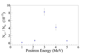
The measured ratio of positron to electron ratio is given the following Table~\ref{tab:e+2e-} and Fig.~\ref{fig:e+2e-}.
\begin{table} \centering \caption{Positron to Electron Rate Ratio.} \begin{tabular}{lc} \toprule {Energy} & {Positron to Electron Ratio} \\ \midrule $1.02 \pm 0.06$ & $(0.19 \pm 0.19)\times10^{-16}$ \\ $2.15 \pm 0.06$ & $(0.69 \pm 0.24)\times10^{-16}$ \\ $3.00 \pm 0.06$ & $(8.25 \pm 0.96)\times10^{-15}$ \\ $4.02 \pm 0.06$ & $(4.20 \pm 0.80)\times10^{-15}$ \\ $5.00 \pm 0.06$ & $(0.62 \pm 0.16)\times10^{-16}$ \\
\bottomrule \end{tabular} \label{tab:e+2e-} \end{table}
\begin{figure} \centering \includegraphics[scale=0.80]{5-Experiment/Figures/Ratio/R.eps} \caption{Ratio of positrons detected to electrons in experiment.} \label{fig:e+2e-} \end{figure}
To find Error on the energy, the 3~MeV electron beam is directed to the phosphorous screen at the end of the 90 degree beamline. The beam centered then steering away from the center by changing the current by $\Delta$I = 0.1 A. This 0.1 A change in the dipole current corresponding to 0.06 MeV differece in the beam energy for 3~MeV beam. For other energies, the it is also 0.06~MeV after rounding up.
%\subsubsection{Error on Ratio} % %Error on electron beam is derived from: % %Error on positron beam rate is derived from: $\sqrt{\frac{positron~rate}{run~time}}$ % %\subsubsection{Annihilation Target Angle} %Use simulation to determine how sensitive annihilation of positrons is to angle. % %What is the dependence of the annihilation target angle with the probability of a positron annihilating in the target and producing a photon that is detected by the NaI detector, % %What is the distribution of 511s as a function of angle phi when theta is 90 degrees? Are they uniformly produced? %\subsubsection{Energy cut systematics} % %How does the positron production efficiency change when you change the range of the 511 cut.
Conclusions and Suggestions
% How to explain simulation does not match experiment. Find the sensitive part went wrong, and say this is went wrong, if we fix it we get the same result. \chapter{Conclusions and Suggestions}
1. HRRL beamline: The HRRL cavity placed to new location. New magnetic elements and diagnostic tolls added to the beamline. HRRL beam successfully reconfigured for positron production and can also generate electron beam with improved quality.
2. Successfully constructed a positron detection system using two NaI detectors, thin tungsten foils a 6-way cross.
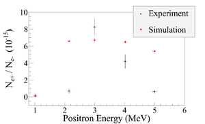
3. Successfully measured positrons at different energies (1 $-$ 5~MeV) in experiment. The ratio of positrons being detected on NaI detectors to electrons incident on T2 is on the order of $10^{-15}$ and peak distribution observed around 3~MeV.
4. In the experiment quarupoles were optimized to transport 2~MeV due to the limited beam time and it could have diminished transportation efficiency for other energies. Further experimental study is necessary to investigate the positron beam energy distribution.
5. Simulation results indicate that the transportation efficiency are varies for different energies. Higher energies has better transportation efficiency. While simulation results agrees with experiment in the peak energy distribution is around 3~MeV, it disagrees with experiment in the ratio of the peak to other energies. %Beam loss
4. Experimental results show quarupole magnet is not efficient in collecting positrons, since positrons have large angular distribution. Solenoid can be used to improve the collection efficiency of positrons~\cite{kim-bindu-solenoid} and should be placed as close the production target as possible for better efficiency.
\begin{figure} \centering \includegraphics[scale=0.80]{6-Conclusion/Figures/Overlay_Exp-Sim-Ratio/R.eps} \caption{Ratio of positrons detected to electrons in experiment and simulation.} \label{fig:e+2e-exp-sim} \end{figure}
List of Figures
 1.1 Form factor ratio, obtained by Rosenbluth Technique (hollow square) and results from Recoil Polarization Technique [5]. . . . . 3
 1.2 Photon generation from Bremsstrahlung processes. . . . . . . . . . . . . . . 4
 1.3 Simulated Bremsstrahlung photon energy right after a tungsten foil. . . . . . 5
 1.4 Simulated electron energy distribution right before a tungsten foil. . . . . . . 6
 1.5 Cross section for each type of photon interaction with tungsten as function of photon energy [10]. . . . . . . . . . . . . . . . 6
 1.6 Pair production. . . . . . . . . . . . . . . . . . . . . . . . . . . . . . . . . . . 8
 1.7 Photon spectrum of 12 MeV mono energy 10 million electrons impinge on a 1.016 mm thick tungsten target. . . . . . . . . . . 8
 1.8 Apparatus used to measure the beam emittance. . . . . . . . . . . . . . . . . 11
 2.1 HRRL cavity. . . . . . . . . . . . . . . . . . . . . . . . . . . . . . . . . . . . 16
 2.2 HRRL beamline layout and parts. . . . . . . . . . . . . . . . . . . . . . . . . 17
300 px 2.3 The OTR Imaging system. . . . . . . . . . . . . . . . . . . . . . . . . . . . . 19
300 px 2.4 Background subtracted to minimize impact of dark current; (a) a beam with the dark current and background noise, (b) a background image, (c) a beam image when dark background was subtracted. . . . . . . . . . . . . . . . . . 21
300 px 2.5 Square of rms values and parabolic fittings. . . . . . . . . . . . . . . . . . . . 23
 2.6 HRRL energy scan (blue dots) and fit (red line) with two skewed Gaussian distribution. . . . . . . . . . . . . . . 25
 2.7 Positron Detection System. T2 (pink) is 45 degree placed with horizontal plane, then rotated towards left detector 45 degree. . . . . . . . . . . 26
 2.8 Modified PMT base design. . . . . . . . . . . . . . . . . . . . . . . . . . . . 28
300 px 2.9 NaI crystal dimension. . . . . . . . . . . . . . . . . . . . . . . . . . . . . . . 29
300 px 2.10 NaI crystals and new bases. . . . . . . . . . . . . . . . . . . . . . . . . . . . 29
 2.11 Pulses from Co-60 source observed on the scope. The amplitude is about 60 mV. The rise time is larger than 50 ns, and the fall time is larger than 700 ns. . . . . . . . .. . . . . . . . . 30
300 px 2.12 Calibrated NaI spectrum of Na-22 and Co-60 sources. . . . . . . . . . . . . . 30
300 px 3.1 T1 is positron production target with same geometry and material as real target. DUPT1 is virtual detector located upstream to sample incoming electron beam. DDNT1 is down stream virtual detector; DT1 is a virtual detector that is placed right after T1 with same angle as T1. . . . . . . . . 34
300 px 3.2 Energy distribution of positrons detected on virtual detector DDNT1. . . . . 35
300 px 3.3 Transverse spacial and angular distribution of positrons on the virtual detector DDNT1. . . . . . . . . . . . . . 36
300 px 3.4 Geometry of the target T1 and the virtual detector DDNT1. . . . . . . . . . 37
300 px 3.5 Positron beam distribution Y divergence vs. Y spacial distribution on DDNT1. 37
300 px 3.6 Positron beam energy distribution detected on the downstream of T2. . . . . 38
300 px 3.7 Step 2 setup. . . . . . . . . . . . . . . . . . . . . . . . . . . . . . . . . . . . 39
 3.8 T2 and virtual detectors located upstream (DT2UP) and downstream (DT2DN) of T2. NaI dettectos and Pb shielding. . . . . . . . . . . 40
 3.9 NaI detector eficiency [21]. . . . . . . . . . . . . . . . . . . . . . . . . . . . 41
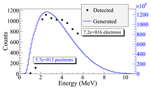 3.10 Positrons generated detected on virtual detector DDNT1 and 511 keV counts
detected by NaI detectors in coincidence mode (100 % eficiency assumed). . 42
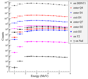 3.11 Predicted number positrons of transported. Black circle: positrons after T1. Red circle: positrons enter Q4. Blue circle: positrons enters D1. Magenta
circle: positrons reaches T2. . . . . . . . . . . . . . . .. . . 42
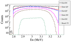 3.12 Beam transported when dipoles are set for 3 MeV positrons. . . . . . . . . . 45
 4.1 Positron detection using T2 and NaI detectors. . . . . . . . . . . . . . . . . . 49
300 px 4.2 T2 in run (red) and T2 out background run (blue) time normalized spectrum. Top row shows original spectrum and bottom row shows incidents only happen in 511 keV peak coincidently on both detectors. . . . . . . . . . . . 50
300 px 4.3 Electron beam monitor. . . . . . . . . . . . . . . . . .. . . . 52
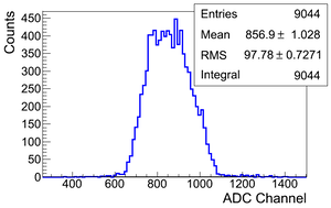 4.4 Electron beam monitor ADC signal . . . . . . . . . . . . . . . . . . . . . . . 52
 4.5 Ratio of positrons detected to electrons in experiment. . . . . . . . . . . . . 55
 5.1 Ratio of positrons detected to electrons in experiment and simulation. . . . . 58