Difference between revisions of "Lab 17 RS"
Jump to navigation
Jump to search
| Line 19: | Line 19: | ||
| Zero-Gate-Voltage Drain Current ||<math> I_{DSS}</math> || 2.0 || 20 || mAdc | | Zero-Gate-Voltage Drain Current ||<math> I_{DSS}</math> || 2.0 || 20 || mAdc | ||
|- | |- | ||
| − | | || <math>V_{GS(off)}</math> || | + | | Gate-Source Cutoff Voltage|| <math>V_{GS(off)}</math> || - || -8.0 || Vdc |
|- | |- | ||
| || <math>P_{max}</math> || || || | | || <math>P_{max}</math> || || || | ||
Revision as of 16:24, 6 April 2011
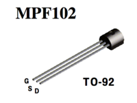
The JFET (Junction Field Effect Transistor n-channel)
File:JFET MPF102 DataSheet.pdf
1.) Complete the table below for the JFET.
| Characteristic | Symbol | Min | Max | Unit |
| Zero-Gate-Voltage Drain Current | 2.0 | 20 | mAdc | |
| Gate-Source Cutoff Voltage | - | -8.0 | Vdc | |
| 3.3 M | ||||
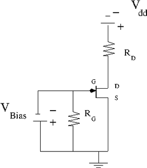
2.)Construct the JFET circuit below.
3.)Plot measurements of -vs- by varying for = 0, 0.5, 1.0, 1.5 V. (40 pnts)
4.)Plot -vs- (30 pnts)
5.)Calculate for your JFET (20 pnts)
Question
- Does depend on? (10 pnts)
Go Back to All Lab Reports Forest_Electronic_Instrumentation_and_Measurement

