Difference between revisions of "TF EIM Chapt5"
Jump to navigation
Jump to search
| Line 8: | Line 8: | ||
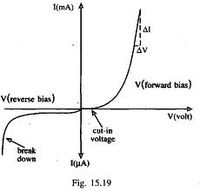
[[File:TF_EIM_Diode_V-vs-I_curve.jpg| 200 px]] | [[File:TF_EIM_Diode_V-vs-I_curve.jpg| 200 px]] | ||
| + | |||
| + | |||
| + | |||
| + | {| border="3" cellpadding="20" cellspacing="0" | ||
| + | |[[File:TF_EIM_ForwardBiased_bottomhalfBipolar.jpg| 400 px]] | ||
| + | |- | ||
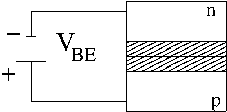
| + | | The n-p junction | ||
| + | |- | ||
| + | |} | ||
=Transistor Physical features= | =Transistor Physical features= | ||
Revision as of 01:54, 6 March 2011
Bipolar Transistor
The Bipolar transistor concept
From the last chapter we saw a p-n junction diode which had similar characteristic current-vs- voltage responses when biased either in the forward direction or backward.

|
| The n-p junction |
Transistor Physical features
The three layers
A transistor has three semi-conductor payers. The three layers occur in the order of
p-n-p= holes-electron-hole
n-p-n= electron-hole-electron
The three layers are formed from a single crystal such that the doping of the single crystal defines the boundaries. The three layers are not "glued" together.
