Difference between revisions of "Forest PMTs"
Jump to navigation
Jump to search
| Line 71: | Line 71: | ||
The figure below has several mistakes in ther region near the capacitors. The Hamamatsu drawing scanned in above is correct.. | The figure below has several mistakes in ther region near the capacitors. The Hamamatsu drawing scanned in above is correct.. | ||
| − | 1.) There should be no line connecting R11 to the anode. The anode goes from the socket (Pin 5) directly to the output connector | + | 1.) There should be no line connecting R11 to the anode. The anode goes from the socket (Pin 5) directly to the output connector. R11 should go to ground as shown. |
2.) Capacitors C1 and C2 should not be going to ground. C1 should be soldered across Resistor R9( in parallel with R9) and C2 should be soldered across Resistor R10. | 2.) Capacitors C1 and C2 should not be going to ground. C1 should be soldered across Resistor R9( in parallel with R9) and C2 should be soldered across Resistor R10. | ||
Latest revision as of 22:31, 19 November 2009
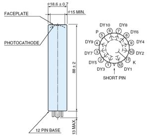
Hamamatsu R4125HA
| Specifications | |
| Part Number | R4125 |
| Type | Head on |
| Size | 19mm |
| ActiveDia/L | 15mm |
| Min | 300nm |
| Max | 650nm |
| Peak Sens. | 420nm |
| Cathode Radiant Sensitivity | 90mA/W |
| Window | Borosilicate |
| Cathode Type | Bialkali |
| Cathode Luminous Sensitivity | 115mA/lm |
| Cathode Blue Sensitivity Index | 11 |
| Anode Luminous Sensitivity | 100A/lm |
| Gain | 8.7E+05 |
| Dark Current after 30 min. | 10nA |
| Rise Time | 2.5ns |
| Transit Time | 16ns |
| Transit Time Spread | 0.85ns |
| Number of Dynodes | 10 |
| Applied Voltage | 1500V |
| Multi Anode | N |
| Magnetic Shield | E989-02 |
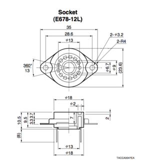
| Socket Bare | E678-12L |
| Socket + bleeder assy. | E974-19 |
| Power Supply | C4840 series |
| Amplifier | C7319 C6438 C5594 M7279 M8879 |
HS Student 2009 summer project
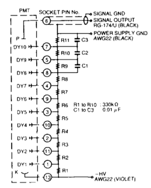
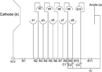
Dynode chain HV design
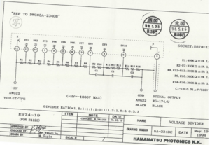
The figure below has several mistakes in ther region near the capacitors. The Hamamatsu drawing scanned in above is correct..
1.) There should be no line connecting R11 to the anode. The anode goes from the socket (Pin 5) directly to the output connector. R11 should go to ground as shown.
2.) Capacitors C1 and C2 should not be going to ground. C1 should be soldered across Resistor R9( in parallel with R9) and C2 should be soldered across Resistor R10.
