Difference between revisions of "Readout Electronics"
| Line 70: | Line 70: | ||
| − | void s3610VFATclock(int id, unsigned int val) | + | void s3610VFATclock(int id, unsigned int val) |
| − | { | + | { |
int i; | int i; | ||
Revision as of 11:40, 3 September 2008
I/O
Inputs to breakout box
- Trigger (LVDS)
- Clock ( RF synced pulse 31 MHz = 499/16 MHz, LVDS)
- Flip Flop scaner (1 TTL pulse)
V1495 :
- 28 Pin output on 34 pin ribbon cables
- Inputs to V1495:
- 180 bits of data = 12 bits Bunch Counter ( =31 MHz clock) + 12 bit (Event Counter + flags) + 12 bits (Chip ID) + 128 bits (data) + 16 bits (Checksum)
- The input register has been set to a size of 256 bit and there are 12 of them
Timing
- VFAT:
- Progammable through the Latency register (8 bits = 256 bits) you have but only 128 registers data registers. We can go back in time 100 *32 ns = 3 micro seconds. But we only may need 100 ns.
V1495: can have programmable delay up to?
We can program delays and play with the timing by downloading values for "lat" into the VFAT extended register and set delay on the V1495 through the ROC.
The V1495 can also interupt the VME backplane telling a ROC to readout the planes.
FPGA to VME data transfer
On 2/15/07 Ben Royd tested the read and write speeds between the VPM backplane and the FPGA user registers. He was able to write 16 bits to USER FPGA in 330 ns.
VFAT controls
Brian Oborn: 282- 6243
VFAT control registers
Control register 0
| bit | bit name | Function |
| 0 | Sleep/Run | 0 = sleep, 1=run also reffereed to as sleep blocking |
Control Register 1
Control register 2
VFAT Clock and Trig pulses
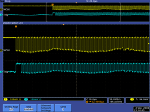
The Clock and Trigger LVDS pusles for the VFAT board were generated using the SIS3610 I/O register. I simply wrote bits to the register. The I/O registers internal clock then determine the pulse frequency. I set the bits to be 1110000000000000 using the command
s3610VFATclock(0,57344);
and reset the highest bit to zero 0110000000000000 b = 16384 d by hardwiring the value int he SIS3610 library function call.
void s3610VFATclock(int id, unsigned int val)
{
int i;
 if((id<0) || (s3610p[id] == NULL)) {
   logMsg("s3610WriteOutput: ERROR : SIS3610 id %d not initialized \n",id,0,0,0,0,0);
   return;
 }
 s3610p[id]->d_out = val;
 s3610p[id]->d_out = 16384;
 s3610p[id]->d_out = val;
 s3610p[id]->d_out = 16384;
 s3610p[id]->d_out = val;
 s3610p[id]->d_out = 16384;
 for(i=0;i<200;i++)
   {
     s3610p[id]->d_out = val;
     s3610p[id]->d_out = 0;
   }
 logMsg("s3610VFATclock: Finish pulses \n",id,0,0,0,0,0);
 return;
}
Cal pulse Procedure
calibrate the circuit response
1.) Connect CalOut to DCU by setting DACsel = 1001
echo "p 65 0 on p 65 1 off p 65 2 off p 65 3 on" | flipbit.arm
2.) set calibration mode to output VCal values by setting CalMode = 01
echo "p 64 6 on p 64 7 off p " | flipbit.arm
3.) set the DAC and monitor how the output changes by setting TrimDAC = a five bit value
For channel 1 set TrimDAC= 1000 ( TrimDAC(4) =1 all others zero)
echo "e 1 1 off e 1 2 off e 1 3 off e 1 4 on" | flipbit.arm
set everything off
echo "e 1 1 off e 1 2 off e 1 3 off e 1 4 off" | flipbit.arm
for channel 128
echo "e 128 4 on" | flipbit.arm
We may need to change the TrimDAC range
echo "e 134 0 on e 134 1 off e 134 2 on" | flipbit.arm
4.) set VCAL
this turns one of the 8 bits to the calibration voltage Vcal (It ranges from 1.074 to 0.877 Volts)
echo "e 129 1 on" | flipbit.arm
5.) send MClock pulses to look at output by using the SIS3610 to output a stream of LVDS pulses to the VFAT and look at DataOut
s3610VFATclock(0,57344);
set injected voltage
- set VCal
