Difference between revisions of "PADC and TDC"
Jump to navigation
Jump to search
| Line 1: | Line 1: | ||
[[UNCL_DAQ_Setup]] | [[UNCL_DAQ_Setup]] | ||
| + | ==PADC address== | ||
| + | [[File:PADC Address.jpg|200 px|PADC VME Adress]] | ||
| + | |||
| + | const PDC_ADDR = 0x200000 | ||
| + | |||
| + | SW1 (Bits 19-16) =0 | ||
| + | |||
| + | SW2 (bits 23-20) =2 | ||
| + | |||
| + | SW1 (bits 27-24) =0 | ||
| + | |||
| + | SW2 (bits 31-28) =0 | ||
| + | |||
| + | |||
| + | == TDC address== | ||
[[File:TDC1290B Address.jpg|200 px]] | [[File:TDC1290B Address.jpg|200 px]] | ||
| + | |||
| + | |||
| + | const C1190_ADDR = 0x210000 | ||
| + | const C1190_OFFSET = 0x10000 | ||
| + | |||
| + | SW1 (Bits 19-16) =1 | ||
| + | |||
| + | SW2 (bits 23-20) =2 | ||
| + | |||
| + | SW1 (bits 27-24) =8 | ||
| + | |||
| + | SW2 (bits 31-28) =0 | ||
| + | |||
[[UNCL_DAQ_Setup]] | [[UNCL_DAQ_Setup]] | ||
Revision as of 22:12, 11 May 2022
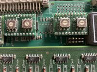
PADC address
const PDC_ADDR = 0x200000
SW1 (Bits 19-16) =0
SW2 (bits 23-20) =2
SW1 (bits 27-24) =0
SW2 (bits 31-28) =0
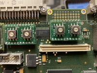
TDC address
const C1190_ADDR = 0x210000
const C1190_OFFSET = 0x10000
SW1 (Bits 19-16) =1
SW2 (bits 23-20) =2
SW1 (bits 27-24) =8
SW2 (bits 31-28) =0

