Difference between revisions of "A W CAA apparatus"
(→NaI) |
|||
| Line 28: | Line 28: | ||
==Geometry== | ==Geometry== | ||
| − | + | Samples were positioned on top of polyethylene blocks. Polyethylene replaced cement blocks to reduce the background. The HpGe detector was suspended from a dewar 9.5 cm above the sample. The NaI detector is perpendicular to the HpGe detector and 6.7 cm from the sample. The NaI detector was shielded using two stand Pb bricks. A drawing of the apparatus is shown in Figure XX.YY. | |
=Signal Processing= | =Signal Processing= | ||
Revision as of 21:04, 14 October 2014
Detectors
HpGe
Type (npn or pnp): Ortec
Model #: SGD-GEM-50180P-S
Bias Voltage: 4600 V POS
Crystal dimensions:
Operating voltage: 5000 V
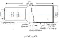
NaI
Type: Bicron
Model #: 3M3/3
Crystal dimensions:
Operating voltage: -1000 V
Geometry
Samples were positioned on top of polyethylene blocks. Polyethylene replaced cement blocks to reduce the background. The HpGe detector was suspended from a dewar 9.5 cm above the sample. The NaI detector is perpendicular to the HpGe detector and 6.7 cm from the sample. The NaI detector was shielded using two stand Pb bricks. A drawing of the apparatus is shown in Figure XX.YY.
Signal Processing
Analog amplification
Discrimination
Signal Trigger logic
Insert you paragraphs describing the apparatus
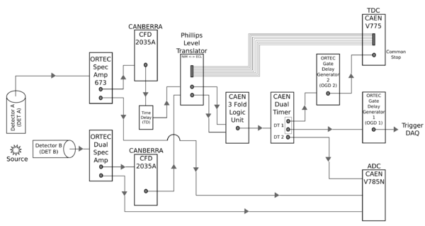
The coincidence counting set-up and modules path are as follows. A source is set atop a base constructed of hydrogen dense blocks. These were chosen to reduce the number of background energy spikes detected. The source is placed an equal distance from decorator A and detector B.
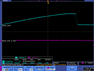
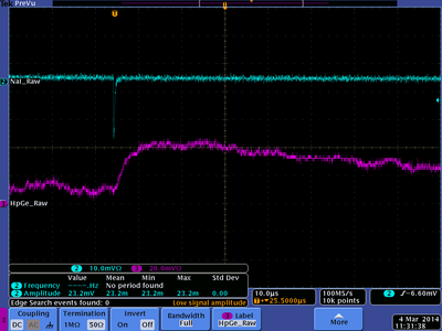
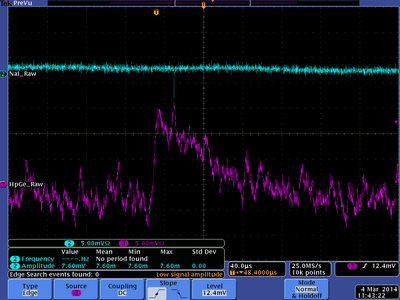
Detector A is positioned directly above the source. A high-purity germanium detector is being utilized for this set-up. The one outgoing signal enters a ORTEC 673 Spectroscopy Amplifier and the outgoing signal then passes through a CANBERRA CFD 2035A. The signal can then enter an optional CAEN CFD to produce a time delay, or can pass directly into a channel (1) of the Level Translator. The second outgoing signal from the Spec Amp goes to a peak sensing CAEN V785N. The output from this module goes to the DAQ.
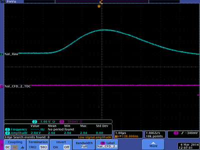
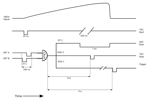
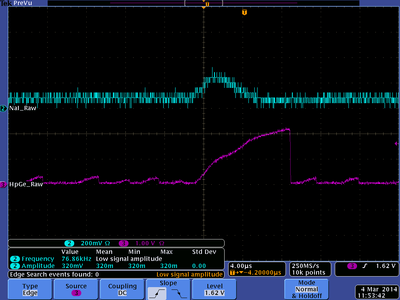
Perpendicular from detector A and placed an equal distance from the source is detector B. This detector can either be a NaI-3 or a germanium detector depending on the source being counted. Detector B’s signal goes to a Post Amplifier and one outgoing signal goes to the above mentioned CAEN V785N and also to the DAQ. The second signal enters a CANBERRA CFD 2035A. The outgoing signal goes to a different channel (4) of the same Level Translator. A ribbon cable on the Level Translator module goes to a Time-to-Digital Converter (TDC) CAEN V775 that is operating in common start mode.
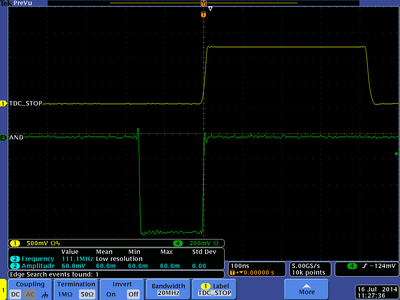
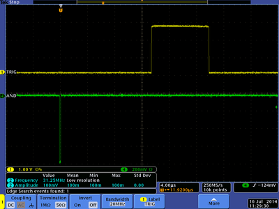
Both channels (1 and 4) of the Level Translator outgoing signal pass to a 3-fold Logic Unit which is used in both OR mode and AND mode to see coincidence lines. This data is collected in the Trig DAQ.
