Difference between revisions of "Lab 23 RS"
| Line 141: | Line 141: | ||
;<math>V_{out}= -\frac{R_2}{R_1} V_1 + \left ( 1 + \frac{R_2}{R_1}\right)V_{io} + R_2 I_B</math> | ;<math>V_{out}= -\frac{R_2}{R_1} V_1 + \left ( 1 + \frac{R_2}{R_1}\right)V_{io} + R_2 I_B</math> | ||
| − | Use the above equation and two measurements of <math>V_{out}</math>, <math>R_1</math>, and <math>R_2</math> to extract <math>V_{io}</math> and <math>I_B</math>. | + | Use the above equation and two measurements of <math>V_{out}</math>, <math>R_1</math>, and <math>R_2</math> to extract <math>V_{io}</math> and <math>I_B</math>. I will use two different values of <math>R_2</math> to make two different measurements. <math> V_{in}</math>=0 (grounded). I can now construct 2 equations with 2 unknowns <math>V_{io}</math> and <math>I_B</math>. |
| − | |||
| − | |||
| − | |||
| − | |||
Revision as of 21:14, 16 April 2011
Inverting OP Amp
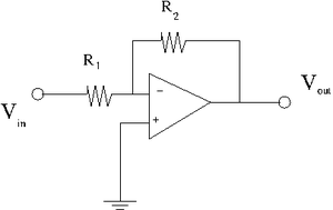
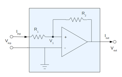
1. Construct the inverting amplifier according to the wiring diagram below.
Here is the data sheet for the 741 Op Amp
Use and as starting values.
2. Insert a 0.1 F capacitor between ground and both Op Amp power supply input pins. The Power supply connections for the Op amp are not shown in the above circuit diagram, check the data sheet.
Gain measurements
1.) Measure the gain as a function of frequency between 100 Hz and 2 MHz for three values of = 10 k, 100 k, 1M. Keep at .
I have used the following values of and (as was suggested by Dr Forrest at the lecture)
a) b) c)
So my theoretical gain of OP Amp would be:
a) Gain1
b) Gain2
c) Gain3
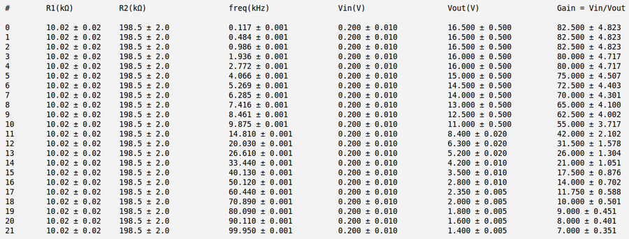
Below is my measurements and gain calculation for the case a) and
Below is my measurements and gain calculation for the case b) and
Below is my measurements and gain calculation for the case c) and
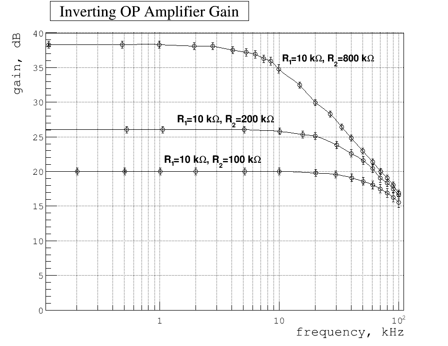
2.) Graph the above measurements with the Gain in units of decibels (dB) and with a logarithmic scale for the frequency axis.
Below my plot of gain as function of frequency. Here
Here the error calculation as usual and for this specific case is:
where and are corresponding gain and error of gain from the tables above
Impedance
Input Impedance
- Measure for the 10 fold and 100 fold amplifier at ~100 Hz and 10 kHz frequency.
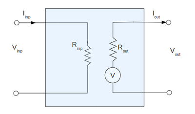
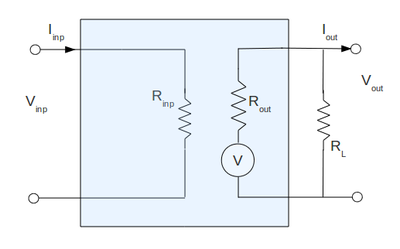
I am going to measure the input and output impedance of my amplifier using the following equivalent circuit:
where the shaded region is my actual amplifier constructed before:
From equivalent circuit the input impedance is:
and from my real circuit inside the shaded region:
so finally my input impedance becomes:
Below is the table with my measurements and input impedance calculations for four asked different cases
As we can see the input impedance equals the resistor value for low frequency and increase up to for high frequency .
Output Impedance
- Measure for the 10 fold and 100 fold amplifier at ~100 Hz and 10 kHz frequency. Be sure to keep the output () undistorted
Again the equivalent circuit I am going to use is:
And my output impedance is:
But now I am going to use the load resistor to measure the output circuit:
By graphing the current on the x-axis and the measured voltage on the y-axis for several values of the load resistance we can find the output internal impedance of our amplifier as the slope of the line
Below is my measurements and current calculation for the case f = 100 Hz, 10 kHz and gain = 10 (here nothing change with frequency)
Below is my measurements and current calculation for the case f = 100 Hz, 10 kHz and gain = 80 (here nothing change with frequency)
As we can see from the tables above my output voltage doesn't change as the current change. It is follow that the slope of the line is zero for all cases and the output impedance is also zero at least for load resistor varying from up to :
and
- (need to be checked)
Use the above equation and two measurements of , , and to extract and . I will use two different values of to make two different measurements. =0 (grounded). I can now construct 2 equations with 2 unknowns and .
Below is my measurements for two different values of .
1) , :
2) , :
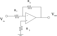
Now we will put in a pull up resistor as shown below.
Instead of the current we have the current
Use the same technique and resistors from the previous section to construct 2 equations and 2 unknowns and extract , keep =0.
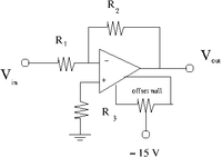
The offset Null Circuit
- Construct the offset null circuit above.
- Adjust the potentiometer to minimize with .
- Use a scope to measure the output noise.
Capacitors
- Revert back to the pull up resistor
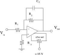
Capacitor in parallel with
- Select a capacitor such that when = 10 kHz.
- Add the capacitor in parallel to so you have the circuit shown above.
- Use a pulse generator to input a sinusoidal voltage
- Measure the Gain as a function of the frequency and plot it.
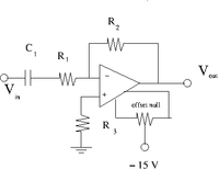
Capacitor in series with R_1
- Select a capacitor such that when = 1 kHz.
- Add the capacitor in series to so you have the circuit shown above.
- Use a pulse generator to input a sinusoidal voltage
- Measure the Gain as a function of the frequency and plot it.
Slew rate
Measure the slew and compare it to the factory spec.
Power Supply Rejection Ratio
- Set V_{in} = 0.
- Measure while changing
Output voltage RMS noise
Go Back to All Lab Reports Forest_Electronic_Instrumentation_and_Measurement
