Difference between revisions of "TF EIM Chapt5"
| Line 20: | Line 20: | ||
| The n-p junction. The depletion region is represented as the shaded square. Notice the depletion region (and E-field in that region) is larger than the forward biased n-p juntion || the potential | | The n-p junction. The depletion region is represented as the shaded square. Notice the depletion region (and E-field in that region) is larger than the forward biased n-p juntion || the potential | ||
|- | |- | ||
| − | |[[File:TF_EIM_BipolarJunction.png| 200 px]][[File:TF_EIM_BipolarJunctionCircuit.png| 200 px]] || | + | |[[File:TF_EIM_BipolarJunction.png| 200 px]][[File:TF_EIM_pnpBipTran.png| 200 px]] [[File:TF_EIM_BipolarJunctionCircuit.png| 200 px]] || |
|- | |- | ||
| The n-p junction. The depletion region is represented as the shaded square. Notice the depletion region (and E-field in that region) is larger than the forward biased n-p juntion || the potential | | The n-p junction. The depletion region is represented as the shaded square. Notice the depletion region (and E-field in that region) is larger than the forward biased n-p juntion || the potential | ||
Revision as of 03:46, 8 March 2011
Bipolar Transistor
The Bipolar transistor concept
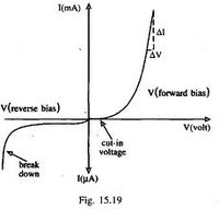
From the last chapter we saw a p-n junction diode which had similar characteristic current-vs- voltage responses when biased either in the forward direction or backward.
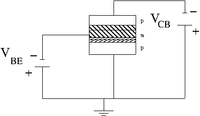
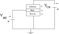
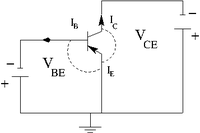
The bottom p-n junction, when forward biased, provides a large current with a small voltage bias.
The top half of the p-n-p transistor is reversed biased, providing a "throttle" for the large current from the lower half.
The electric field points to the "collector" in the depletion region enlarged by the reverse bias. This moves the majority charge carriers away from the collector-base junction. Once outside the depletion zone, the charge carriers rely on diffusion to escape the material..
Transistor Physical features
The three layers
A transistor has three semi-conductor payers. The three layers occur in the order of
p-n-p= holes-electron-hole
n-p-n= electron-hole-electron
The three layers are formed from a single crystal such that the doping of the single crystal defines the boundaries. The three layers are not "glued" together.


