Difference between revisions of "PhotoFiss 3-4-11"
Jump to navigation
Jump to search
| Line 67: | Line 67: | ||
=Scope Pictures= | =Scope Pictures= | ||
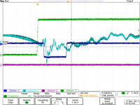
| − | Below is a picture of a FC pixel and the ADC integrate gate used to measure the charge deposited on that pixel during the gate. The picture was taken just before run | + | Below is a picture of a FC pixel and the ADC integrate gate used to measure the charge deposited on that pixel during the gate. The picture was taken just before run 1831. |
The 40 mV amplitude pulse is shown on top of the RF noise. The pulse is produced by a XXX ns wide electron pulse containing a peak current of YYYY mA. | The 40 mV amplitude pulse is shown on top of the RF noise. The pulse is produced by a XXX ns wide electron pulse containing a peak current of YYYY mA. | ||
Revision as of 21:28, 5 March 2011
TDC Map
| TDC Chan | Detector |
| 1 | Event Trigger |
| 12 | Sofiia (neutron detector Beam Right down) |
| 13 | Natali (neutron detector Beam Left down) |
| 14 | Irina (neutron detector Beam left center) |
| 15 | Polina (neutron detector Beam left top) |
Runs
| Date | Run Number | Comment |
| 3/4/11 | 1831 | 25 MeV FC test, see scope picture #46 |
| 3/4/11 | 1832 | FC test, 3mm vertical Al collimation in front of FC |
| 3/4/11 | 1834 | FC 9V battery test on each channel |
| 3/4/11 | 1835 | FC test with beam-on same results as run 1832 |
| 3/4/11 | 1836 | FC test bending beam down with 0-100A |
| 3/4/11 | 1837-47 | FC Calibration beam down 10A step size (need to move FC up) |
| 3/4/11 | 1848-57 | FC Calibration beam down 10A step size |
| 3/4/11 | 1858-67 | FC Calibration beam up 10A step size |
| 3/4/11 | 1868-9 | Dr. Dale's collimation, no results laying Al bricks horizontally |
| 3/4/11 | 1870 | Dr. Dale's collimation, weird results |
| 3/4/11 | 1871-2 | Dr. Dale's collimation works |
| 3/4/11 | 1873-5 | Wedged Dr. Dale's collimation and swept beam using kickers |
| 3/4/11 | 1877-99 | Kicker Magnet calibration using view screen |
| 3/4/11 | ||
| 3/4/11 | ||
| 3/4/11 | ||
| 3/4/11 | ||
| 3/4/11 | ||
| 3/4/11 |
Scope Pictures
Below is a picture of a FC pixel and the ADC integrate gate used to measure the charge deposited on that pixel during the gate. The picture was taken just before run 1831.
The 40 mV amplitude pulse is shown on top of the RF noise. The pulse is produced by a XXX ns wide electron pulse containing a peak current of YYYY mA.
