Difference between revisions of "A W CAA apparatus"
| (78 intermediate revisions by 2 users not shown) | |||
| Line 29: | Line 29: | ||
| − | The second detector employed in our coincidence set-up was a Sodium Iodide (NaI) detector. NaI detectors are a type of scintillation detector usually coupled to a photomultiplier tube (PMT). The NaI scintillator material is doped with thallium and fluoresces when excited by ionizing radiation. The thallium is used to increase the probability for photon emission. The emitted light strikes a photocathode, releasing at most one photoelectron per photon. The ejected electron is accelerated towards a system dynodes by an electric field. Additional electrons are knocked off each stage of the dynode as a result of the applied electric field resulting in a measurable signal that is collected at the anode and coupled to a coaxial BNC output connector. We used a Bicron model 3M3/3 detector with a <math>3 \times 3</math> inch crystal. The PMT voltage was set at -1000 V. A picture of the detector and its diagram can be seen on figures XX.YY and XX.YY. | + | The second detector employed in our coincidence set-up was a Sodium Iodide (NaI) detector. NaI detectors are a type of scintillation detector usually coupled to a photomultiplier tube (PMT). The NaI scintillator material is doped with thallium and fluoresces when excited by ionizing radiation. The thallium is used to increase the probability for photon emission. The emitted light strikes a photocathode, releasing at most one photoelectron per photon. The ejected electron is accelerated towards a system of dynodes by an electric field. Additional electrons are knocked off each stage of the dynode as a result of the applied electric field resulting in a measurable signal that is collected at the anode and coupled to a coaxial BNC output connector. We used a Bicron model 3M3/3 detector with a <math>3 \times 3</math> inch crystal. The PMT voltage was set at -1000 V. A picture of the detector and its diagram can be seen on figures XX.YY and XX.YY. |
| Line 39: | Line 39: | ||
Samples were positioned on top of polyethylene blocks. Polyethylene replaced cement blocks to reduce the background from the cement blocks. The HpGe detector was suspended from a dewar 9.5 cm above the sample. The NaI detector is perpendicular to the HpGe detector and 6.7 cm from the sample. The NaI detector was shielded using two standard (2x4x8 inch) Pb bricks. A drawing of the apparatus is shown in Figure XX.YY. | Samples were positioned on top of polyethylene blocks. Polyethylene replaced cement blocks to reduce the background from the cement blocks. The HpGe detector was suspended from a dewar 9.5 cm above the sample. The NaI detector is perpendicular to the HpGe detector and 6.7 cm from the sample. The NaI detector was shielded using two standard (2x4x8 inch) Pb bricks. A drawing of the apparatus is shown in Figure XX.YY. | ||
| − | [[File: | + | [[File:GeometryDiagram_2.png || 400 px]][[File:DetectorGeo_picture.png || 200 px]] |
=Signal Processing= | =Signal Processing= | ||
| Line 45: | Line 45: | ||
==Analog output== | ==Analog output== | ||
| − | As seen in the HpGe detector diagram Fig. ZZZ.PPa, the charge carriers from the crystal are sent directly to a preamplifier, which converts the charge pulse from the detector to a voltage. This positive voltage signal has a rise time 8 microseconds and a decay time of 60-80 microseconds with an amplitude of | + | As seen in the HpGe detector diagram Fig. ZZZ.PPa, the charge carriers from the crystal are sent directly to a preamplifier, which converts the charge pulse from the detector to a voltage. This positive voltage signal has a rise time 8 microseconds and a decay time of 60-80 microseconds with an amplitude of 40 mV as shown in figureXX.YY. The signal is next sent to a post amplifier that provides a voltage gain to bring the pulse amplitude to 1.75 V where it can more conveniently be processed. |
| − | The NaI detector | + | The NaI detector PMT output is shown in figureXX.YY. In contrast to the HpGe signal, the negative voltage NaI signal has a pulse width of 2-3 microseconds and an amplitude between 5 and 10 mV. An inverting amplifier was used to convert the signal to a positive amplitude and broaden the pulse with a gradually rounded maximum peak amplitude of 640 mV. The signal is also more symmetric. The amplified signal can be seen alongside the HpGe amplified signal in figureXX.YY. |
| Line 54: | Line 54: | ||
==Analog amplification== | ==Analog amplification== | ||
| + | |||
| + | [[File:Detector Diagram_8.png | 600 px]] | ||
| + | |||
| + | FigureXX.YY is a diagram of the modules used for the coincidence experiment. Detector B is positioned directly above the source and corresponds to our HpGe detector as mentioned in the set-up geometry section above. The pre-amplified signal of the HpGe detector is post amplified by an ORTEC 673 Spectroscopy Amplifier. The adjustable controls where set to the following values: The Spec-Amp course grain was x20, the fine grain dial was set to x1.04 for an overall gain of x20.8, and the sharpening time to 0.25<math>\mu</math>sec. The BLR switch was in the auto position and the input switch in the positive position. The time variant gated integrator (GI) output from the Spec Amp goes to a Peak Sensing Analog-to-Digital Converter (PADC). The unipolar (UNI) output continues to a Constant Fraction Discriminator (CFD). | ||
| + | |||
| + | A NaI detector, Detector A, is shown in FigureXX.YY. The NaI detector's analog signal also passes through a post amplifier. We used an Ortec 855 Dual Spectroscopy Amplifier in our set-up. The course gain dial was set to x20 and the fine gain dial was set to x8.98 for an overall gain of x179.6. The outgoing signals were sent from the BI output to a CFD and the UNI output to the PADC. | ||
==Discrimination== | ==Discrimination== | ||
| − | == | + | For our experiment we used two Canberra 2035A Constant Fraction Timing SCA which performed both energy and timing analysis on post amplified analog pulses. The amplitude of the analog signal is typically proportional to the energy a photon deposits in the detector. Low energy background events are reduced using the discriminator. Both CFD modules where set to accept 60 keV photons or greater. The output logic pulse from this constant fraction discriminator occurs at the same point in the rise of input pulse. To accomplish this, the analog pulse into the discriminator is superimposed onto a copy of that input that has been inverted, attenuated, and offset in time. Adding the two signals yields a bipolar signal. A timing discriminator triggers on the zero-crossing of the signal, producing an output logic pulse. After the CFD, one pulse, with a pulse width of 20 ns, went straight to the a time-to-digital converter (TDC start). A copy of that same pulse went to two gate generators that where used to increase the pulse widths to 100 ns. This increase in the width of the logic pulse corresponds to a 200 ns timing window for coincidence events. In other words, a coincidence is thought to exist if the two output signals occur within 200 seconds of each other. |
| + | |||
| + | |||
| + | [[File:Canberra2037A.pdf]] | ||
| + | |||
| + | ==DAQ readout timing== | ||
| + | |||
| + | |||
| + | |||
| + | {| border="1" |cellpadding="20" cellspacing="0 | ||
| + | |- | ||
| + | | [[File:Signal_Diagram_3.png | 600 px]] | ||
| + | |- | ||
| + | | Timing Diagram:<math> t_{stop}=600 ns</math>, <math>t_{trig}= 13 \mu s</math> | ||
| + | |- | ||
| + | |} | ||
| + | |||
| + | The output of the coincidence logic unit is used to trigger the data acquisition system. The trigger was sent into a CAEN Dual Timer with multiple outputs. One output was given a fixed delay (<math>t_{stop}</math>) with an ORTEC Gate Delay Generator before going to the common stop of the TDC. A second timed pulse, one microsecond wide, was sent to the PADC gate. The analog output from the post amplifiers is delayed in time. This delay was of sufficient length that the amplified analog output was in time with the coincidence logic pulse used start a measurement in the PADC. A copy of that same timed pulse went through a separate gate delay of <math>t_{trig}</math> and used to signal the DAQ that data was ready to be readout of the VME modules. The trigger was delayed to allow time for the DAQ to convert the analog signals to digital signals. A diagram of these signals, their widths, and their timing can be seen in FigureXX.YY. | ||
| + | ==Coincidence timing electronics== | ||
| + | [[File:TDC7023_1.png | 400 px]] | ||
| − | |||
| + | A false coincidence background can be suppressed further by requiring simultaneous signals from both detectors. The 20 ns wide logic pulses produced by the CFD are sent to a time-to-digital converter (TDC) and to a logic unit, after their width has been increase to 100 ns as shown in FigureXX.YY. The logic unit will compare the timing pulses in an AND gate that only provides output if the two pulses are within a 200 nanosecond window. The coincidence output is used to open a linear gate that signals the PADC to look for a peak within a 1 usec window. FigureXX.YY is a plot of the time difference between the two detector pulses thought to be in coincidence. It shows the expected timing window of +/- 100 ns. We estimate the probability of having an false coincidence by dividing the number of accidental background event using the number of real coincidence events. The probability of an accidental event was approximately 10.19% for a best case scenario and approximately 24.81% for a worst case scenario. | ||
| + | ==Calibrating Detectors== | ||
| + | |||
| + | [[File:Ba133_raw.png | 400 px]] | ||
| + | [[File:Ba133_cal_2.png | 400 px]] | ||
| − | |||
| − | + | {| border="1" |cellpadding="20" cellspacing="0 | |
| + | |- | ||
| + | | Ba-133 Coincidence Photon Energies (keV)|| HpGe Energies Before Calibration (keV) | ||
| + | |- | ||
| + | | 80.9971 || 220.9 +/- 1.81 | ||
| + | |- | ||
| + | | 276.3997|| 546.6 +/- 1.87 | ||
| + | |- | ||
| + | | 302.8510|| 590.5 +/- 1.67 | ||
| + | |- | ||
| + | | 356.0134|| 678.9 +/- 1.52 | ||
| + | |- | ||
| + | | 383.8480|| 725.1 +/- 1.71 | ||
| + | |- | ||
| + | |} | ||
| + | The detectors are calibrated using standard sources of Cs-137, Co-60, Na-22, Ba-133, and Mn-54. The certificates for these sources along with their coincidence photon energies are be located in Appendix X. Each source was counted in singles mode until the number of events had exceeded 100,000. The mean and sigma of each energy peak was recorded and these values along with the known photon energies where fit to a linear function. Table XX.YY gives Ba-133 known energies in column 1 along with an example of the energies before calibration given by the HpGe detector. The parameters of the fit where applied to calibrate the detectors. FigureXX.YY shows the Ba-133 energy spectrum before and after the detector was calibrated. The long term variance in detector calibration parameters over the course of experiment and the impact of energy calibration drift is analyzed in sectionXX.YY, "Energy calibration systematic error." | ||
| − | + | =Scope Images= | |
| − | |||
| − | [[File: | + | [[File:NaI_HpGe_RAW_Coin_3_4_2014.png | 400 px]] |
| + | [[File:NaI_HpGe_RAW_Coin_3_4_2014_zoomed.png | 400 px]] | ||
| − | |||
| + | [[File:NaI_HpGe_DFD_to_TDC_Coin_3_4_2014.png | 400 px]] | ||
| − | |||
| − | [[File: | + | [[File:HpGe_DFD_to_TDC_Coin_3_4_2014.png | 400 px]] |
| − | |||
| − | + | [[File:HpGe_TDCstop.png | 400 px]] | |
| − | |||
| − | + | [[File:HpGe_Trig.png | 400 px]] | |
Latest revision as of 15:37, 28 October 2014
Detectors
HpGe
Type (npn or pnp): Ortec
Model #: SGD-GEM-50180P-S
Crystal dimensions: active diameter 65 mm (6.5 cm)
Operating voltage: 4600 V
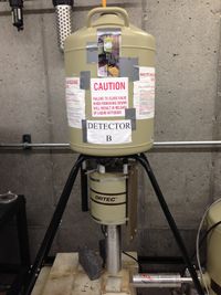
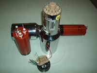
A high-purity germanium (HpGe) detector is the first of two detectors used in for our coincidence set-up. These detectors employ a germanium semiconductor to measure the energy of impinging radiation. In semiconductor detectors, the incident photon's energy is measured by the number of charge carriers set free in the material's valence band and transferred to the conduction band. An equal number of electronic vacancies or "holes" are created in the valance band. Placing the material between two electrodes and applying an electric field will give a measurable pulse. In order to reduce thermal excitations of valence electrons, the detector is cooled to liquid nitrogen temperatures. HpGe detectors have an energy resolution of 1 keV. We used a p-type germanium from Ortec model SGD-GEM-50180P-S with an active crystal diameter of 65 mm. The 4600 V detector bias was controlled by the SMART-INTERFACE computer software. FigureXX.YY shows the detector with a dewar attached that kept the detector cool for at least one week before additional nitrogen was required.
NaI
Type: Bicron
Model #: 3M3/3
Crystal dimensions: inches ( cm)
Operating voltage: -1000 V
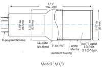
The second detector employed in our coincidence set-up was a Sodium Iodide (NaI) detector. NaI detectors are a type of scintillation detector usually coupled to a photomultiplier tube (PMT). The NaI scintillator material is doped with thallium and fluoresces when excited by ionizing radiation. The thallium is used to increase the probability for photon emission. The emitted light strikes a photocathode, releasing at most one photoelectron per photon. The ejected electron is accelerated towards a system of dynodes by an electric field. Additional electrons are knocked off each stage of the dynode as a result of the applied electric field resulting in a measurable signal that is collected at the anode and coupled to a coaxial BNC output connector. We used a Bicron model 3M3/3 detector with a inch crystal. The PMT voltage was set at -1000 V. A picture of the detector and its diagram can be seen on figures XX.YY and XX.YY.
Geometry
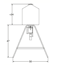
Samples were positioned on top of polyethylene blocks. Polyethylene replaced cement blocks to reduce the background from the cement blocks. The HpGe detector was suspended from a dewar 9.5 cm above the sample. The NaI detector is perpendicular to the HpGe detector and 6.7 cm from the sample. The NaI detector was shielded using two standard (2x4x8 inch) Pb bricks. A drawing of the apparatus is shown in Figure XX.YY.
Signal Processing
Analog output
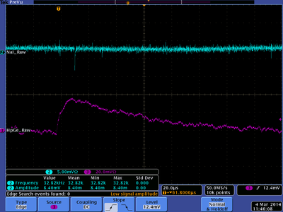
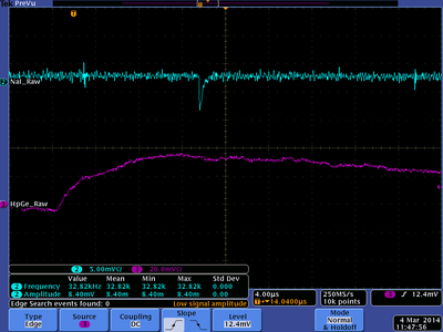
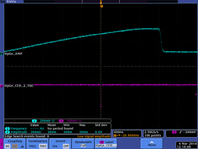
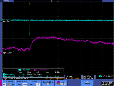
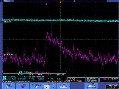
As seen in the HpGe detector diagram Fig. ZZZ.PPa, the charge carriers from the crystal are sent directly to a preamplifier, which converts the charge pulse from the detector to a voltage. This positive voltage signal has a rise time 8 microseconds and a decay time of 60-80 microseconds with an amplitude of 40 mV as shown in figureXX.YY. The signal is next sent to a post amplifier that provides a voltage gain to bring the pulse amplitude to 1.75 V where it can more conveniently be processed.
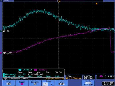
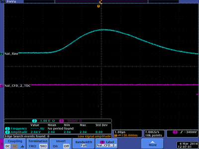
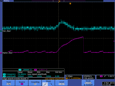
The NaI detector PMT output is shown in figureXX.YY. In contrast to the HpGe signal, the negative voltage NaI signal has a pulse width of 2-3 microseconds and an amplitude between 5 and 10 mV. An inverting amplifier was used to convert the signal to a positive amplitude and broaden the pulse with a gradually rounded maximum peak amplitude of 640 mV. The signal is also more symmetric. The amplified signal can be seen alongside the HpGe amplified signal in figureXX.YY.
Analog amplification
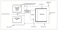
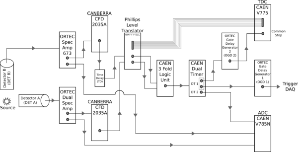
FigureXX.YY is a diagram of the modules used for the coincidence experiment. Detector B is positioned directly above the source and corresponds to our HpGe detector as mentioned in the set-up geometry section above. The pre-amplified signal of the HpGe detector is post amplified by an ORTEC 673 Spectroscopy Amplifier. The adjustable controls where set to the following values: The Spec-Amp course grain was x20, the fine grain dial was set to x1.04 for an overall gain of x20.8, and the sharpening time to 0.25sec. The BLR switch was in the auto position and the input switch in the positive position. The time variant gated integrator (GI) output from the Spec Amp goes to a Peak Sensing Analog-to-Digital Converter (PADC). The unipolar (UNI) output continues to a Constant Fraction Discriminator (CFD).
A NaI detector, Detector A, is shown in FigureXX.YY. The NaI detector's analog signal also passes through a post amplifier. We used an Ortec 855 Dual Spectroscopy Amplifier in our set-up. The course gain dial was set to x20 and the fine gain dial was set to x8.98 for an overall gain of x179.6. The outgoing signals were sent from the BI output to a CFD and the UNI output to the PADC.
Discrimination
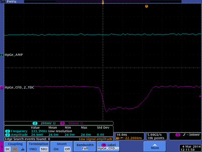
For our experiment we used two Canberra 2035A Constant Fraction Timing SCA which performed both energy and timing analysis on post amplified analog pulses. The amplitude of the analog signal is typically proportional to the energy a photon deposits in the detector. Low energy background events are reduced using the discriminator. Both CFD modules where set to accept 60 keV photons or greater. The output logic pulse from this constant fraction discriminator occurs at the same point in the rise of input pulse. To accomplish this, the analog pulse into the discriminator is superimposed onto a copy of that input that has been inverted, attenuated, and offset in time. Adding the two signals yields a bipolar signal. A timing discriminator triggers on the zero-crossing of the signal, producing an output logic pulse. After the CFD, one pulse, with a pulse width of 20 ns, went straight to the a time-to-digital converter (TDC start). A copy of that same pulse went to two gate generators that where used to increase the pulse widths to 100 ns. This increase in the width of the logic pulse corresponds to a 200 ns timing window for coincidence events. In other words, a coincidence is thought to exist if the two output signals occur within 200 seconds of each other.
DAQ readout timing
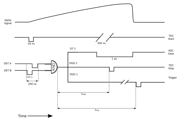
|
| Timing Diagram:, |
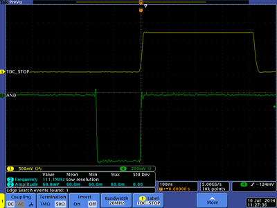
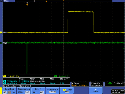
The output of the coincidence logic unit is used to trigger the data acquisition system. The trigger was sent into a CAEN Dual Timer with multiple outputs. One output was given a fixed delay () with an ORTEC Gate Delay Generator before going to the common stop of the TDC. A second timed pulse, one microsecond wide, was sent to the PADC gate. The analog output from the post amplifiers is delayed in time. This delay was of sufficient length that the amplified analog output was in time with the coincidence logic pulse used start a measurement in the PADC. A copy of that same timed pulse went through a separate gate delay of and used to signal the DAQ that data was ready to be readout of the VME modules. The trigger was delayed to allow time for the DAQ to convert the analog signals to digital signals. A diagram of these signals, their widths, and their timing can be seen in FigureXX.YY.
Coincidence timing electronics
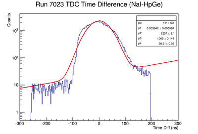
A false coincidence background can be suppressed further by requiring simultaneous signals from both detectors. The 20 ns wide logic pulses produced by the CFD are sent to a time-to-digital converter (TDC) and to a logic unit, after their width has been increase to 100 ns as shown in FigureXX.YY. The logic unit will compare the timing pulses in an AND gate that only provides output if the two pulses are within a 200 nanosecond window. The coincidence output is used to open a linear gate that signals the PADC to look for a peak within a 1 usec window. FigureXX.YY is a plot of the time difference between the two detector pulses thought to be in coincidence. It shows the expected timing window of +/- 100 ns. We estimate the probability of having an false coincidence by dividing the number of accidental background event using the number of real coincidence events. The probability of an accidental event was approximately 10.19% for a best case scenario and approximately 24.81% for a worst case scenario.
Calibrating Detectors
| Ba-133 Coincidence Photon Energies (keV) | HpGe Energies Before Calibration (keV) |
| 80.9971 | 220.9 +/- 1.81 |
| 276.3997 | 546.6 +/- 1.87 |
| 302.8510 | 590.5 +/- 1.67 |
| 356.0134 | 678.9 +/- 1.52 |
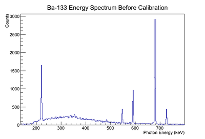
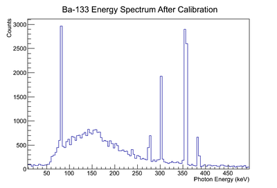
| 383.8480 | 725.1 +/- 1.71 |
The detectors are calibrated using standard sources of Cs-137, Co-60, Na-22, Ba-133, and Mn-54. The certificates for these sources along with their coincidence photon energies are be located in Appendix X. Each source was counted in singles mode until the number of events had exceeded 100,000. The mean and sigma of each energy peak was recorded and these values along with the known photon energies where fit to a linear function. Table XX.YY gives Ba-133 known energies in column 1 along with an example of the energies before calibration given by the HpGe detector. The parameters of the fit where applied to calibrate the detectors. FigureXX.YY shows the Ba-133 energy spectrum before and after the detector was calibrated. The long term variance in detector calibration parameters over the course of experiment and the impact of energy calibration drift is analyzed in sectionXX.YY, "Energy calibration systematic error."
Scope Images
