Difference between revisions of "Lab 23 RS"
| (189 intermediate revisions by the same user not shown) | |||
| Line 6: | Line 6: | ||
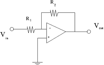
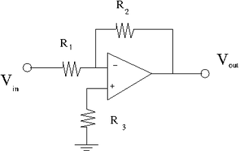
1. Construct the inverting amplifier according to the wiring diagram below. | 1. Construct the inverting amplifier according to the wiring diagram below. | ||
| − | [[File:TF_EIM_Lab23.png| | + | [[File:TF_EIM_Lab23.png| 350 px]] |
Here is the data sheet for the 741 Op Amp | Here is the data sheet for the 741 Op Amp | ||
| Line 25: | Line 25: | ||
<math>R_1 = (10.02 \pm 0.02)\ k\Omega</math> | <math>R_1 = (10.02 \pm 0.02)\ k\Omega</math> | ||
| − | + | <math>a)\ R_2 = (99.0 \pm 0.2)\ k\Omega</math> | |
| − | + | <math>b)\ R_2 = (198.5 \pm 0.2)\ k\Omega</math> | |
| − | + | <math>c)\ R_2 = (800.0 \pm 2.0)\ k\Omega</math> | |
So my theoretical gain of OP Amp would be: | So my theoretical gain of OP Amp would be: | ||
| − | + | <math>a)\ \mbox{Gain}_1 = \frac{R_2}{R_1} = \frac{99.0 \pm 0.2}{10.02 \pm 0.02} = (9.88 \pm 0.03)</math> | |
| − | + | <math>b)\ \mbox{Gain}_2 = \frac{R_2}{R_1} = \frac{198.5 \pm 0.2}{10.02 \pm 0.02} = (19.81 \pm 0.04)</math> | |
| − | + | <math>c)\ \mbox{Gain}_3 = \frac{R_2}{R_1} = \frac{800.0 \pm 2.0}{10.02 \pm 0.02} = (79.84 \pm 0.26)</math> | |
Below is my measurements and gain calculation for the case a) <math>R_1 = (10.02 \pm 0.02)\ k\Omega</math> and <math>R_2 = (99.0 \pm 0.2)\ k\Omega</math> | Below is my measurements and gain calculation for the case a) <math>R_1 = (10.02 \pm 0.02)\ k\Omega</math> and <math>R_2 = (99.0 \pm 0.2)\ k\Omega</math> | ||
| − | [[File: | + | [[File:Gain t01.png | 900px]] |
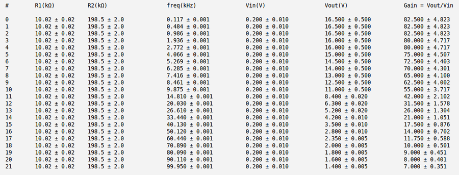
Below is my measurements and gain calculation for the case b) <math>R_1 = (10.02 \pm 0.02)\ k\Omega</math> and <math>R_2 = (198.5 \pm 0.2)\ k\Omega</math> | Below is my measurements and gain calculation for the case b) <math>R_1 = (10.02 \pm 0.02)\ k\Omega</math> and <math>R_2 = (198.5 \pm 0.2)\ k\Omega</math> | ||
| − | [[File: | + | [[File:Gain t02.png | 900px]] |
Below is my measurements and gain calculation for the case c) <math>R_1 = (10.02 \pm 0.02)\ k\Omega</math> and <math>R_2 = (800.0 \pm 2.0)\ k\Omega</math> | Below is my measurements and gain calculation for the case c) <math>R_1 = (10.02 \pm 0.02)\ k\Omega</math> and <math>R_2 = (800.0 \pm 2.0)\ k\Omega</math> | ||
| − | [[File: | + | [[File:Gain t03.png | 900px]] |
| Line 56: | Line 56: | ||
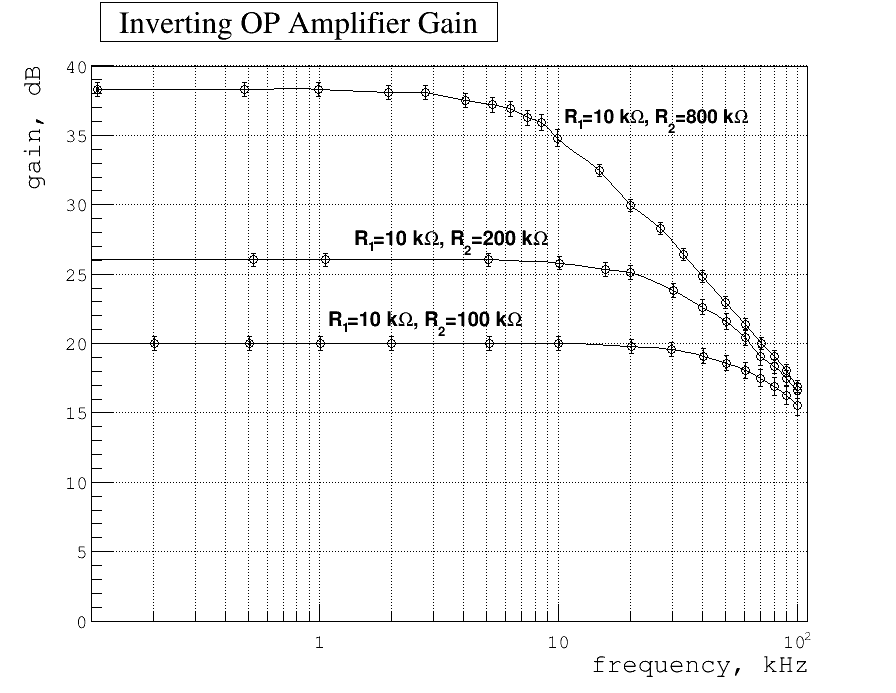
| − | Below my plot of gain as function of frequency. Here | + | Below my plot of gain as function of frequency. Here are: |
<math>G_{dB} \left(\frac{V_{out}}{V_{in}}\right) = 20\cdot \log_{10} {\frac{V_{out}}{V_{in}}}</math> | <math>G_{dB} \left(\frac{V_{out}}{V_{in}}\right) = 20\cdot \log_{10} {\frac{V_{out}}{V_{in}}}</math> | ||
| − | + | The error propagation is as usual and for this specific case is: | |
<math>dG_{dB}(x) = \frac{\partial G_{dB}(x)}{\partial x}\cdot dx = \frac{20}{x\ \ln 10}\cdot dx</math> | <math>dG_{dB}(x) = \frac{\partial G_{dB}(x)}{\partial x}\cdot dx = \frac{20}{x\ \ln 10}\cdot dx</math> | ||
| Line 73: | Line 73: | ||
#Measure <math>R_{in}</math> for the 10 fold and 100 fold amplifier at ~100 Hz and 10 kHz frequency. | #Measure <math>R_{in}</math> for the 10 fold and 100 fold amplifier at ~100 Hz and 10 kHz frequency. | ||
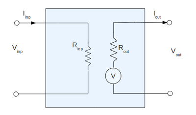
| − | + | I am going to measure the input and output impedance of my total amplifier (because I think it is what was asked) using the following equivalent circuit: | |
| − | I am going to measure the input and output impedance of my amplifier using the following equivalent circuit: | ||
[[File:Draw01.png | 400px]] | [[File:Draw01.png | 400px]] | ||
| Line 95: | Line 94: | ||
| − | Below is the table with my measurements and input impedance calculations for four asked different cases | + | Below is the table with my measurements and input impedance calculations for four asked different cases. Here I have used the meter instead of oscilloscope to reduce the error in my measurements of input voltage (so the measured values of voltage are RMS) |
| − | [[File: | + | [[File:t_rinp01.png | 800px]] |
| − | As we can see the input impedance equals the resistor value <math>R_1</math> for low frequency <math>f=100\ Hz</math> and increase up to <math>33\ k\Omega</math> for high frequency <math>f=10\ kHz</math>. | + | As we can see the input impedance equals the resistor value <math>R_1</math> for low frequency <math>f=100\ Hz</math> and increase up to <math>33\ k\Omega</math> for high frequency <math>f=10\ kHz</math> and for high gain 80. I would like to note here that calculated above input impedance values are for the total amplifier circuit and are not just for chip alone. The input impedance of chip alone is very high (about 1 <math>M\Omega</math> for bipolar OP AMP) and very difficult to measure because of very small input voltage and current values at both input terminals of the chip. |
==Output Impedance== | ==Output Impedance== | ||
| Line 121: | Line 120: | ||
| − | Below | + | Below are my measurements and current calculation for different cases. Here I have used the meter instead of oscilloscope to reduce the error in my measurements of output voltage (so the measured voltage values are RMS) |
| − | [[File: | + | [[File:t_rout01.png | 800px]] |
| − | |||
| − | + | Below are the plots of the <math>V_{out}</math> as function of <math>I_{out}</math> | |
| − | + | [[File:p_rout_00.png | 1050 px]] | |
| − | |||
| − | = <math> | + | As it follows from the plots above the output impedance (the slope of the line) are: |
| + | |||
| + | 1) 10 fold amplifier at ~100 Hz frequency: <math>R_{out} = (8.68\cdot 10^{-11} \pm 112.3)\ \Omega</math> | ||
| + | 2) 10 fold amplifier at ~10 kHz frequency: <math>R_{out} = (6.70\cdot 10^{-11} \pm 120.4)\ \Omega</math> | ||
| + | 3) 80 fold amplifier at ~100 Hz frequency: <math>R_{out} = (-1.65\cdot 10^{-11} \pm 136.7)\ \Omega</math> | ||
| + | 3) 80 fold amplifier at ~10 kHz frequency: <math>R_{out} = (8.35\cdot 10^{-11} \pm 218.8)\ \Omega</math> | ||
| − | + | As we can see the output impedance is essentially the zero. Unfortunately the calculated error is up to <math>220.\ \Omega</math>. To get the better results I need dramatically improve my measurements, and particularly, improve the measured error in <math>V_{out}</math> | |
| + | = <math>V_{io}</math> and <math>I_{B}</math>= | ||
| − | ;<math>V_{out}= -\frac{R_2}{R_1} | + | ;<math>V_{out}= -\frac{R_2}{R_1} V_{in} + \left ( 1 + \frac{R_2}{R_1}\right)V_{io} + R_2 I_B</math> |
Use the above equation and two measurements of <math>V_{out}</math>, <math>R_1</math>, and <math>R_2</math> to extract <math>V_{io}</math> and <math>I_B</math>. I will use two different values of <math>R_2</math> to make two different measurements. <math> V_{in}</math>=0 (grounded). | Use the above equation and two measurements of <math>V_{out}</math>, <math>R_1</math>, and <math>R_2</math> to extract <math>V_{io}</math> and <math>I_B</math>. I will use two different values of <math>R_2</math> to make two different measurements. <math> V_{in}</math>=0 (grounded). | ||
| − | Below are my measurements | + | Below are my measurements. I have used the meter instead of oscilloscope to reduce my measured error in measured small output voltage. |
| − | 1) <math>f=1 kHz</math> <math>R_1 = (10. | + | 1) <math>f=1\ kHz</math> <math>R_1 = (10.06 \pm 0.01)\ k\Omega</math>, <math>R_2 = (99.5 \pm 0.1)\ k\Omega</math>: <math>V_{in}=(0.05 \pm 0.05)\ mV</math> <math>V_{out}=(6.9 \pm 0.05)\ mV</math> |
| − | + | 2) <math>f=1\ kHz</math> <math>R_1 = (10.06 \pm 0.01)\ k\Omega</math>, <math>R_2 = (199.6 \pm 0.1)\ k\Omega</math>: <math>V_{in}=(0.05 \pm 0.05)\ mV</math> <math>V_{out}=(14.1 \pm 0.05)\ mV</math> | |
| − | 2) <math>f=1 kHz</math> <math>R_1 = (10. | ||
Now I can construct 2 equations with 2 unknowns <math>V_{io}</math> and <math>I_B</math>. | Now I can construct 2 equations with 2 unknowns <math>V_{io}</math> and <math>I_B</math>. | ||
| − | :<math> (1 + (99. | + | :<math> (1 + (99.5 \pm 0.1)/(10.06 \pm 0.01))\cdot V_{io} + (99.5 \pm 0.1)\ k\Omega \cdot I_B = (6.9 \pm 0.05)\ mV</math> |
| − | :<math> (1 + ( | + | :<math> (1 + (199.6 \pm 0.1)/(10.06 \pm 0.01))\cdot V_{io} + (199.6 \pm 0.1)\ k\Omega \cdot I_B = (14.1 \pm 0.05)\ mV</math> |
or | or | ||
| − | :<math> 10. | + | :<math> (10.891 \pm 0.014)\cdot V_{io} + (99.5 \pm 0.1)\cdot 10^3\ I_B = (6.9 \pm 0.05)\cdot 10^{-3}</math> |
| − | :<math> | + | :<math> (20.841 \pm 0.022)\cdot V_{io} + (199.6 \pm 0.1)\cdot 10^3\ I_B =(14.1 \pm 0.05)\cdot 10^{-3}</math> |
| + | |||
| + | with <math>V_{io}</math> given in Volts and <math>I_B</math> given in Amperes. | ||
| − | To solve these | + | To solve these equations will use the matrix method. Let's do it in general to be able to handle the error propagation. We have: |
:<math>\left( \begin{array}{cc} a_1 & b_1\\ a_2 & b_2 \end{array} \right)\left( \begin{array}{c} V_{io} \\ I_B \end{array} \right) = \left( \begin{array}{c} c_1 \\ c_2 \end{array} \right)</math> | :<math>\left( \begin{array}{cc} a_1 & b_1\\ a_2 & b_2 \end{array} \right)\left( \begin{array}{c} V_{io} \\ I_B \end{array} \right) = \left( \begin{array}{c} c_1 \\ c_2 \end{array} \right)</math> | ||
| − | the two solutions are: | + | and the two solutions are: |
| + | |||
| + | : <math>V_{io} = \frac{\left| \begin{array}{cc} c_1 & b_1\\c_2 & b_2 \end{array} \right| }{\left| \begin{array}{cc} a_1 & b_1\\a_2 & b_2 \end{array} \right| } = \frac{c_1b_2-c_2b_1}{a_1b_2-a_2b_1}\ \ </math>: <math>I_B = \frac{\left| \begin{array}{cc} a_1 & c_1\\a_2 & c_2 \end{array} \right| }{\left| \begin{array}{cc} a_1 & b_1\\a_2 & b_2 \end{array} \right| } = \frac{a_1c_2-a_2c_1}{a_1b_2-a_2b_1}</math> | ||
| + | |||
| + | |||
| + | Substituting the corresponding coefficients: | ||
| − | : <math> | + | : <math>V_{io} = \frac{c_1b_2-c_2b_1}{a_1b_2-a_2b_1} = \frac{(6.9 \pm 0.05)\cdot 10^{-3}\cdot (199.6 \pm 0.1)\cdot 10^3 - (14.1 \pm 0.05)\cdot 10^{-3}\cdot (99.5 \pm 0.1)\cdot 10^3}{(10.891 \pm 0.014)\cdot (199.6 \pm 0.1)\cdot 10^3 - (20.841 \pm 0.022)\cdot (99.5 \pm 0.1)\cdot 10^3}</math> |
| + | : <math>I_B = \frac{a_1c_2-a_2c_1}{a_1b_2-a_2b_1} = \frac{(10.891 \pm 0.014)\cdot (14.1 \pm 0.05)\cdot 10^{-3} - (20.841 \pm 0.022)\cdot (6.9 \pm 0.05)\cdot 10^{-3}}{(10.891 \pm 0.014)\cdot (199.6 \pm 0.1)\cdot 10^3 - (20.841 \pm 0.022)\cdot (99.5 \pm 0.1)\cdot 10^3}</math> | ||
| − | + | and by doing math and handling the error propagation we find: | |
| − | + | <math>V_{io} = (-0.257 \pm 0.114)\ mV </math> | |
| + | <math>I_B = (97.5 \pm 12.0)\ nA </math> | ||
= <math>I_{io}</math>= | = <math>I_{io}</math>= | ||
| − | Now we will put in a pull up resistor <math>R_3= \frac{R_1 R_2}{R_1+R_2}</math> as shown below. | + | Now we will put in a pull up resistor <math>R_3= \frac{R_1 R_2}{R_1+R_2}</math>(measured) as shown below. |
| + | |||
| + | I have constructed <math>R_3</math> from two resistor in parallel identical to my <math>R_1</math> and <math>R_2</math> used in my initial circuit. | ||
| − | [[File:TF_EIM_Lab23a.png | | + | a) <math>R_3= (10\ k\Omega)||(100\ k\Omega) = (9.20 \pm 0.01)\ k\Omega</math>(measured) |
| + | b) <math>R_3= (10\ k\Omega)||(200\ k\Omega) = (9.66 \pm 0.01)\ k\Omega</math>(measured) | ||
| + | |||
| + | [[File:TF_EIM_Lab23a.png | 350 px]] | ||
Instead of the current <math>I_B</math> we have the current <math>I_{io}</math> | Instead of the current <math>I_B</math> we have the current <math>I_{io}</math> | ||
| − | ;<math>V_{out}= -\frac{R_1}{ | + | ;<math>V_{out}= -\frac{R_2}{R_1} V_{in} + \left ( 1 + \frac{R_2}{R_1}\right)V_{io} + R_2 I_{io}</math> |
| + | |||
Use the same technique and resistors from the previous section to construct 2 equations and 2 unknowns and extract <math>I_{io}</math>, keep <math>V_{in}</math>=0. | Use the same technique and resistors from the previous section to construct 2 equations and 2 unknowns and extract <math>I_{io}</math>, keep <math>V_{in}</math>=0. | ||
| + | |||
| + | |||
| + | Below are my measurements. I have used the meter instead of oscilloscope to reduce my measured error in measured small output voltage. <math>f=1\ kHz</math>. | ||
| + | |||
| + | 1) <math>R_1 = (10.06\pm0.01)\ k\Omega</math>,<math>R_2 = (99.5\pm0.1)\ k\Omega</math>,<math>R_3 = (9.20\pm0.01)\ k\Omega</math>: <math>V_{in}=(0.05 \pm 0.05)\ mV</math>,<math>V_{out}=(-1.5 \pm 0.05)\ mV</math> | ||
| + | 2) <math>R_1 = (10.06\pm0.01)\ k\Omega</math>,<math>R_2 = (199.6\pm0.1)\ k\Omega</math>,<math>R_3 = (9.20\pm0.01)\ k\Omega</math>: <math>V_{in}=(0.05 \pm 0.05)\ mV</math>,<math>V_{out}=(-2.8 \pm 0.05)\ mV</math> | ||
| + | |||
| + | and to equations becomes: | ||
| + | |||
| + | :<math> (10.891 \pm 0.014)\cdot V_{io} + (99.5 \pm 0.1)\cdot 10^3\ I_{io} = (-1.5 \pm 0.05)\cdot 10^{-3}</math> | ||
| + | :<math> (20.841 \pm 0.022)\cdot V_{io} + (199.6 \pm 0.1)\cdot 10^3\ I_{io} =(-2.8 \pm 0.05)\cdot 10^{-3}</math> | ||
| + | |||
| + | with <math>V_{io}</math> given in Volts and <math>I_B</math> given in Amperes. | ||
| + | |||
| + | |||
| + | Substituting the corresponding coefficients into general solutions derived above: | ||
| + | |||
| + | : <math>V_{io} = \frac{c_1b_2-c_2b_1}{a_1b_2-a_2b_1} = \frac{(-1.5 \pm 0.05)\cdot 10^{-3}\cdot (199.6 \pm 0.1)\cdot 10^3 - (-2.8 \pm 0.05)\cdot 10^{-3}\cdot (99.5 \pm 0.1)\cdot 10^3}{(10.891 \pm 0.014)\cdot (199.6 \pm 0.1)\cdot 10^3 - (20.841 \pm 0.022)\cdot (99.5 \pm 0.1)\cdot 10^3}</math> | ||
| + | |||
| + | : <math>I_{io} = \frac{a_1c_2-a_2c_1}{a_1b_2-a_2b_1} = \frac{(10.891 \pm 0.014)\cdot (-2.8 \pm 0.05)\cdot 10^{-3} - (20.841 \pm 0.022)\cdot (-1.5 \pm 0.05)\cdot 10^{-3}}{(10.891 \pm 0.014)\cdot (199.6 \pm 0.1)\cdot 10^3 - (20.841 \pm 0.022)\cdot (99.5 \pm 0.1)\cdot 10^3}</math> | ||
| + | |||
| + | and by doing math and handling the error propagation we find: | ||
| + | |||
| + | <math>V_{io} = (-0.208 \pm 0.112)\ mV </math> | ||
| + | <math>I_{io} = (7.7 \pm 11.2)\ nA </math> | ||
| + | |||
| + | |||
| + | So by properly choosing the resistor values <math>R_3</math> I was able to reduce my input offset current <math>I_{io}</math> from about <math>100\ nA</math> (case without <math>R_3</math>) down to about <math>8\ nA</math> (case with <math>R_3</math>). By doing that I did my amplifier more perfect (input current for perfect OP AMP is zero). Unfortunately my error for <math>I_{io}</math> becomes compared with the calculated values of the quantity by itself. But that is because the used method was (the error really comes from the solution of equations). Probably using different method to calculate <math>I_{io}</math>, for example using scope to measure input voltage and current, we can reduce the measured error. But even with error calculated above we can clearly see the relative reductions of the input offset circuit. | ||
= The offset Null Circuit= | = The offset Null Circuit= | ||
| − | [[File:TF_EIM_Lab23_b.png | | + | [[File:TF_EIM_Lab23_b.png | 350 px]] |
| + | |||
| + | 1) Construct the offset null circuit above. | ||
| + | |||
| + | I have used the gain 20 case with resistors values from previous section: | ||
| + | |||
| + | <math>R_1 = (10.06\pm0.01)\ k\Omega</math>, <math>R_2 = (199.6\pm0.1)\ k\Omega</math>, <math>R_3 = (9.20\pm0.01)\ k\Omega</math> | ||
| + | |||
| + | 2) Adjust the potentiometer to minimize <math>V_{out}</math> with <math>V_{in}=0</math>. | ||
| + | |||
| + | 3) Use a scope to measure the output noise. | ||
| + | |||
| + | My initial values of <math>V_{out}</math> was <math>V_{out}=(-2.8 \pm 0.05)\ mV</math>. Using potentiometer I was able to reduce my <math>V_{out}</math> up to zero values. Basically doing that I have reduced my input offset voltage <math>V_{io}</math> so my amplifier becomes more perfect. | ||
| + | |||
| + | My measured output noise at this point becomes: | ||
| + | |||
| + | <math>(\Delta V_{out})_{RMS} = \frac{1.0\ mV}{2\sqrt{2}} = 0.35\ mV</math> | ||
| − | + | It's difficult to see the noise reduction because my relative compensation of <math>V_{out}</math> was small. But if I will start with big initial <math>V_{out}</math> (for example by adjusting potentiometer) we can observe that noise becomes smaller as we reduce the absolute value of <math>V_{out}</math> | |
| − | |||
| − | |||
= Capacitors= | = Capacitors= | ||
| Line 201: | Line 260: | ||
==Capacitor in parallel with <math>R_2</math>== | ==Capacitor in parallel with <math>R_2</math>== | ||
| − | [[File:TF_EIM_Lab23_c.png | | + | [[File:TF_EIM_Lab23_c.png | 350 px]] |
| + | |||
| + | 1) Select a capacitor such that <math>\frac{1}{\omega C_2} \approx R_2</math> when <math>\omega</math>= 10 kHz. | ||
| + | |||
| + | <math>C_2 \geq \frac{1}{\omega R_2} = \frac{1}{2\pi\times 10\ kHz\times 199.6\ k\Omega} \approx 80 \ pF </math> | ||
| + | |||
| + | I will pick up: | ||
| + | |||
| + | <math>C_2 = 100\ pF</math> | ||
| + | |||
| + | so my break point becomes: | ||
| + | |||
| + | <math>f = \frac{1}{2\pi R_2 C_2} = \frac{1}{2\pi\times 199.6\ k\Omega\times 100\ pF} = 8.0\ kHz</math> | ||
| + | |||
| + | 2) Add the capacitor in parallel to <math>R_2</math> so you have the circuit shown above. | ||
| + | 3) Use a pulse generator to input a sinusoidal voltage <math>V_{in}</math> | ||
| + | 4) Measure the Gain as a function of the <math>V_{in}</math> frequency and plot it. | ||
| + | |||
| + | Below my measured voltages and gain calculation. | ||
| + | |||
| + | [[File:Table gain c2 01.png | 1000 px]] | ||
| + | |||
| + | |||
| + | Below my plot of gain as function of frequency. Also I overplay here my previous measurements of gain without capacitor <math>C_2</math>. | ||
| + | |||
| + | [[File:Plot gain c2.png | 1000 px]] | ||
| + | |||
| + | As we can see the gain are dropping down at about calculated above frequency. It's can be easily understood. At this point the capacitor <math>C_2</math> starts to conduct AC signal reducing the effective resistors <math>R_2</math> value. So at hight frequency the gain = <math>\frac{R_2}{R_1}</math> starts to drop below the usual value without capacitor. It's sometimes very useful because by decreasing the gain at high frequencies we can prevent unwanted possible oscillations at this point , | ||
| + | |||
| + | ==Capacitor in series with <math>R_1</math>== | ||
| + | |||
| + | [[File:TF_EIM_Lab23_d.png | 350 px]] | ||
| + | |||
| + | 1) Select a capacitor such that<math> \frac{1}{\omega C_1} \approx R_1</math> when <math>\omega</math>= 1 kHz. | ||
| + | |||
| + | |||
| + | <math>C_1 \approx \frac{1}{\omega R_1} = \frac{1}{2\pi\times 1\ kHz\times 10.0\ k\Omega} \approx 16 \ nF </math> | ||
| + | |||
| + | I will pick up: | ||
| + | |||
| + | <math>C_1 = 15\ nF</math> (can compose like 10nF || (10nF + 10nF)) | ||
| + | |||
| + | and my break point becomes: | ||
| + | |||
| + | <math>f = \frac{1}{2\pi R_2 C_2} = \frac{1}{2\pi\times 10.0\ k\Omega\times 15\ nF} = 1.06\ kHz</math> | ||
| + | |||
| + | 2) Add the capacitor in series to <math>R_1</math> so you have the circuit shown above. | ||
| + | |||
| + | 3) Use a pulse generator to input a sinusoidal voltage <math>V_{in}</math> | ||
| + | |||
| + | 4) Measure the Gain as a function of the <math>V_{in}</math> frequency and plot it. | ||
| + | |||
| + | Below my measurements and gain calculation: | ||
| + | |||
| + | [[File:Table gain c1.png | 1000 px]] | ||
| + | |||
| − | + | Below my plot of gain as function of frequency. Also I overplay here my previous measurements of gain without capacitor <math>C_1</math>. | |
| − | |||
| − | |||
| − | |||
| − | + | [[File:plot gain c1.png | 1000 px]] | |
| − | |||
| − | + | As we can see the gain starts to go up at about 1 kHz, reaches maximum at about 7 kHz and then goes down. It can be understood as follow. At break point frequency calculated above the capacitor <math></math> starts to conduct the AC signal very well. So we are effectively reduce the <math>R_1</math> resistor values and as follow increase the gain = <math>\frac{R_2}{R_1}</math>. As frequency goes up the competing process of decreasing gain starts to work. And at some point the total gain starts to go down. | |
| − | |||
| − | |||
| − | |||
=Slew rate= | =Slew rate= | ||
Measure the slew and compare it to the factory spec. | Measure the slew and compare it to the factory spec. | ||
| + | |||
| + | Below is the table with my measurements and calculated Slew Rate. I did these measurements for several high frequency points. My input signal was squared wave and I increased the input voltage until I observed the squared wave was transformed to triangle wave so I can measure the Slew Rate as the slope of line: | ||
| + | |||
| + | [[File:SlewRate.png | 500 px]] | ||
| + | |||
| + | |||
| + | <math>SR = \frac{\Delta V}{\Delta t}</math> | ||
| + | |||
| + | |||
| + | [[File:Table sr 01.png | 800 px]] | ||
| + | |||
| + | My best estimate for measured Slew Rate is: | ||
| + | |||
| + | <math>SR = (0.585 \pm0.002)\ \frac{V}{\mu s}</math> | ||
| + | |||
| + | From the data sheet the typical slew rate values for LM741 is: | ||
| + | |||
| + | <math>SR = 0.5\ \frac{V}{\mu s}</math>. | ||
| + | |||
| + | Because it's the typical values and probably varies from one chip to other I think my measured values of slew rate is reasonable and in agreement with data sheet for this type of OP AMP | ||
=Power Supply Rejection Ratio= | =Power Supply Rejection Ratio= | ||
| − | #Set V_{in} = 0. | + | #Set <math>V_{in}</math> = 0. |
| − | #Measure <math>V_{out}</math> while changing <math>V_{cc}</math> | + | #Measure <math>V_{out}</math> while changing <math>V_{cc}</math> |
| + | |||
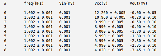
| + | Below are my measurements of <math>V_{out}</math> as function <math>V_{cc}</math> (and I used the <math>R_1 = (10.06\pm0.01)\ k\Omega</math> and <math>R_2 = (199.6\pm0.1)\ k\Omega</math>): | ||
| + | |||
| + | [[File:Table PSRR 02.png | 550 px]] | ||
| + | |||
| + | Below is my plot of <math>V_{out}</math> as function <math>V_{cc}</math>: | ||
| + | |||
| + | [[File:Plot PSRR 02.png | 800 px]] | ||
| + | |||
| + | |||
| + | The experimental points was approximated by polynomial as: | ||
| + | |||
| + | <math>V_{out} = p_0 + p_1 V_{cc} + p_2 V_{cc}^2 + p_3 V_{cc}^3</math> | ||
| + | |||
| + | where | ||
| + | |||
| + | <math>V_{out}\ \mbox{given}\ \mbox{in}\ \mbox{mV}</math> | ||
| + | <math>V_{cc}\ \mbox{given}\ \mbox{in}\ \mbox{V}</math> | ||
| + | <math>p_0 = (-5.711\pm 1.063)</math> | ||
| + | <math>p_1 = (0.5173\pm 0.4342)</math> | ||
| + | <math>p_0 = (0.02024\pm 0.05517)</math> | ||
| + | <math>p_0 = (-0.001992\pm1.002202)</math> | ||
| + | |||
| + | |||
| + | The power supply rejection ratio (PSRR) can be calculated by | ||
| + | |||
| + | <math>PSRR = \frac{1}{\mbox{Gain}}\frac{\Delta V_{out}}{\Delta V_{cc}} = \frac{1}{R_2/R_1}\frac{\partial V_{out}}{\partial V_{cc}} </math> | ||
| + | |||
| + | |||
| + | Using the polynomial above | ||
| + | |||
| + | <math>PSRR = \frac{1}{R_2/R_1}(p_1 + 2\cdot p_2 V_{cc} + 3\cdot p_3 V_{cc}^2)\ \frac{mV}{V}</math> | ||
| + | |||
| + | and substituting the corresponding coefficients and evaluating the PSRR at point <math>V_{cc} = 13\ V</math> (the data sheet values of PSRR is given at <math>V_{cc} = \pm 15\ V</math>, but I can not really evaluate my PSRR at this point because my fitting procedure and my measured values are out of this point): | ||
| + | |||
| + | <math>PSRR = \frac{1}{(199.6\pm0.1)/(10.06\pm0.01)}((0.5173\pm 0.4342) + 2 (0.02024\pm 0.05517)\cdot 13 + 3 (-0.001992\pm1.002202)\cdot 13^2)\ \frac{mV}{V}</math> | ||
| + | |||
| + | By doing math and handling the error propagation we get finally: | ||
| + | |||
| + | <math>PSRR = (1.7\pm 94)\ \frac{uV}{V} = (-204\pm 11280)\ dB </math> | ||
| + | |||
| + | As we can see the calculated PSRR values is pretty close to data sheet typical values of -96 dB (at <math>\pm 15\ V</math>). Unfortunately my error is too high. One way to handle it would be to improve the error of measured small quantities of output voltage. The other way would be to improve the method used to analyze the experimental points, especially find the better approximation function with smaller fitting errors. Also I really need the power supply able to give the varying voltage at about <math>V_{cc}=\pm 15\ V</math> so I can make the corresponding comparison with data sheet value. | ||
=Output voltage RMS noise <math>\Delta V_{out}^{RMS}</math>= | =Output voltage RMS noise <math>\Delta V_{out}^{RMS}</math>= | ||
| + | My measured peak-to-peak noise <math>\Delta V_{out}^{RMS}</math> with <math>V_{in}</math> grounded is: | ||
| + | |||
| + | <math>\mbox{Noise}_{\mbox{peak-to-peak}} = (6\pm0.5)\ mV</math> | ||
| + | So my RMS noise is: | ||
| + | <math>\mbox{Noise}_{\mbox{RMS}} = \frac{(6\pm0.5)\ mV}{2\ \sqrt{2}} = (2.12\pm0.18)\ mV</math> | ||
[https://wiki.iac.isu.edu/index.php/Electronics_RS Go Back to All Lab Reports] [[Forest_Electronic_Instrumentation_and_Measurement]] | [https://wiki.iac.isu.edu/index.php/Electronics_RS Go Back to All Lab Reports] [[Forest_Electronic_Instrumentation_and_Measurement]] | ||
Latest revision as of 14:16, 27 April 2011
Inverting OP Amp
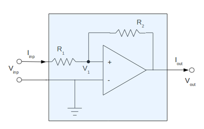
1. Construct the inverting amplifier according to the wiring diagram below.
Here is the data sheet for the 741 Op Amp
Use and as starting values.
2. Insert a 0.1 F capacitor between ground and both Op Amp power supply input pins. The Power supply connections for the Op amp are not shown in the above circuit diagram, check the data sheet.
Gain measurements
1.) Measure the gain as a function of frequency between 100 Hz and 2 MHz for three values of = 10 k, 100 k, 1M. Keep at .
I have used the following values of and (as was suggested by Dr Forrest at the lecture)
So my theoretical gain of OP Amp would be:
Below is my measurements and gain calculation for the case a) and
Below is my measurements and gain calculation for the case b) and
Below is my measurements and gain calculation for the case c) and
2.) Graph the above measurements with the Gain in units of decibels (dB) and with a logarithmic scale for the frequency axis.
Below my plot of gain as function of frequency. Here are:
The error propagation is as usual and for this specific case is:
where and are corresponding gain and error of gain from the tables above
Impedance
Input Impedance
- Measure for the 10 fold and 100 fold amplifier at ~100 Hz and 10 kHz frequency.
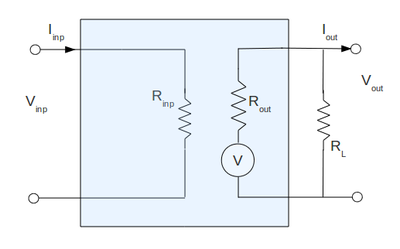
I am going to measure the input and output impedance of my total amplifier (because I think it is what was asked) using the following equivalent circuit:
where the shaded region is my actual amplifier constructed before:
From equivalent circuit the input impedance is:
and from my real circuit inside the shaded region:
so finally my input impedance becomes:
Below is the table with my measurements and input impedance calculations for four asked different cases. Here I have used the meter instead of oscilloscope to reduce the error in my measurements of input voltage (so the measured values of voltage are RMS)
As we can see the input impedance equals the resistor value for low frequency and increase up to for high frequency and for high gain 80. I would like to note here that calculated above input impedance values are for the total amplifier circuit and are not just for chip alone. The input impedance of chip alone is very high (about 1 for bipolar OP AMP) and very difficult to measure because of very small input voltage and current values at both input terminals of the chip.
Output Impedance
- Measure for the 10 fold and 100 fold amplifier at ~100 Hz and 10 kHz frequency. Be sure to keep the output () undistorted
Again the equivalent circuit I am going to use is:
And my output impedance is:
But now I am going to use the load resistor to measure the output circuit:
By graphing the current on the x-axis and the measured voltage on the y-axis for several values of the load resistance we can find the output internal impedance of our amplifier as the slope of the line
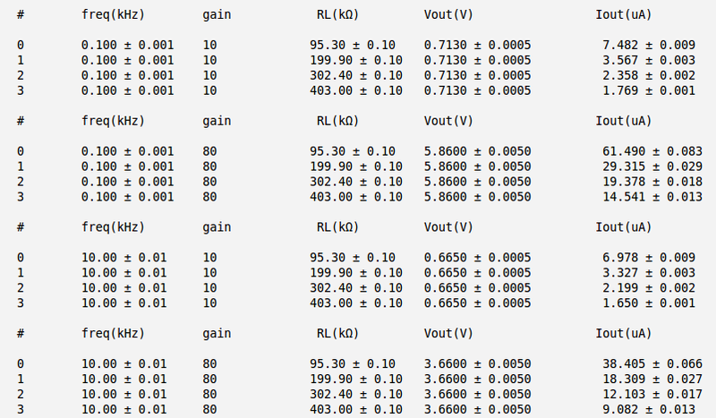
Below are my measurements and current calculation for different cases. Here I have used the meter instead of oscilloscope to reduce the error in my measurements of output voltage (so the measured voltage values are RMS)
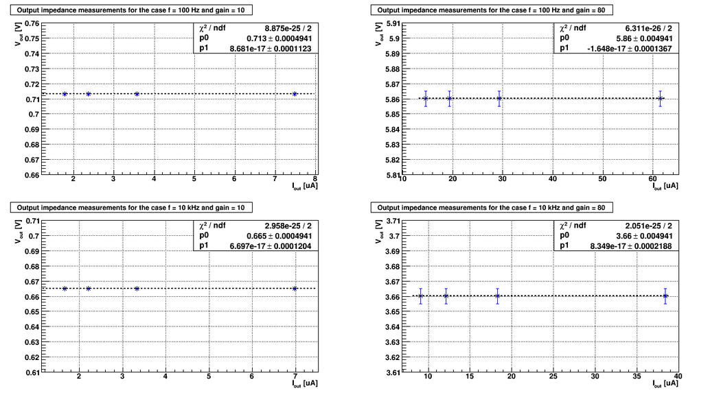
Below are the plots of the as function of
As it follows from the plots above the output impedance (the slope of the line) are:
1) 10 fold amplifier at ~100 Hz frequency: 2) 10 fold amplifier at ~10 kHz frequency: 3) 80 fold amplifier at ~100 Hz frequency: 3) 80 fold amplifier at ~10 kHz frequency:
As we can see the output impedance is essentially the zero. Unfortunately the calculated error is up to . To get the better results I need dramatically improve my measurements, and particularly, improve the measured error in
and
Use the above equation and two measurements of , , and to extract and . I will use two different values of to make two different measurements. =0 (grounded).
Below are my measurements. I have used the meter instead of oscilloscope to reduce my measured error in measured small output voltage.
1) , : 2) , :
Now I can construct 2 equations with 2 unknowns and .
or
with given in Volts and given in Amperes.
To solve these equations will use the matrix method. Let's do it in general to be able to handle the error propagation. We have:
and the two solutions are:
- :
Substituting the corresponding coefficients:
and by doing math and handling the error propagation we find:
Now we will put in a pull up resistor (measured) as shown below.
I have constructed from two resistor in parallel identical to my and used in my initial circuit.
a) (measured) b) (measured)
Instead of the current we have the current
Use the same technique and resistors from the previous section to construct 2 equations and 2 unknowns and extract , keep =0.
Below are my measurements. I have used the meter instead of oscilloscope to reduce my measured error in measured small output voltage. .
1) ,,: , 2) ,,: ,
and to equations becomes:
with given in Volts and given in Amperes.
Substituting the corresponding coefficients into general solutions derived above:
and by doing math and handling the error propagation we find:
So by properly choosing the resistor values I was able to reduce my input offset current from about (case without ) down to about (case with ). By doing that I did my amplifier more perfect (input current for perfect OP AMP is zero). Unfortunately my error for becomes compared with the calculated values of the quantity by itself. But that is because the used method was (the error really comes from the solution of equations). Probably using different method to calculate , for example using scope to measure input voltage and current, we can reduce the measured error. But even with error calculated above we can clearly see the relative reductions of the input offset circuit.
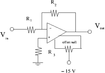
The offset Null Circuit
1) Construct the offset null circuit above.
I have used the gain 20 case with resistors values from previous section:
, ,
2) Adjust the potentiometer to minimize with .
3) Use a scope to measure the output noise.
My initial values of was . Using potentiometer I was able to reduce my up to zero values. Basically doing that I have reduced my input offset voltage so my amplifier becomes more perfect.
My measured output noise at this point becomes:
It's difficult to see the noise reduction because my relative compensation of was small. But if I will start with big initial (for example by adjusting potentiometer) we can observe that noise becomes smaller as we reduce the absolute value of
Capacitors
- Revert back to the pull up resistor
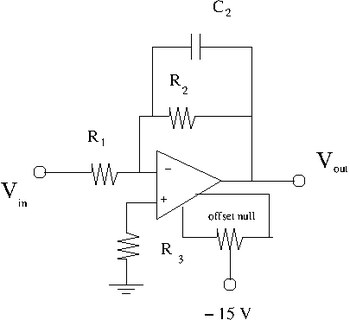
Capacitor in parallel with
1) Select a capacitor such that when = 10 kHz.
I will pick up:
so my break point becomes:
2) Add the capacitor in parallel to so you have the circuit shown above. 3) Use a pulse generator to input a sinusoidal voltage 4) Measure the Gain as a function of the frequency and plot it.
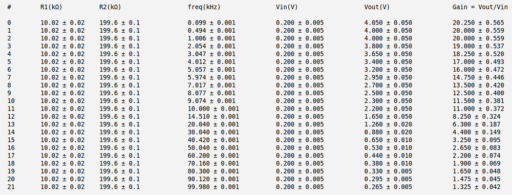
Below my measured voltages and gain calculation.
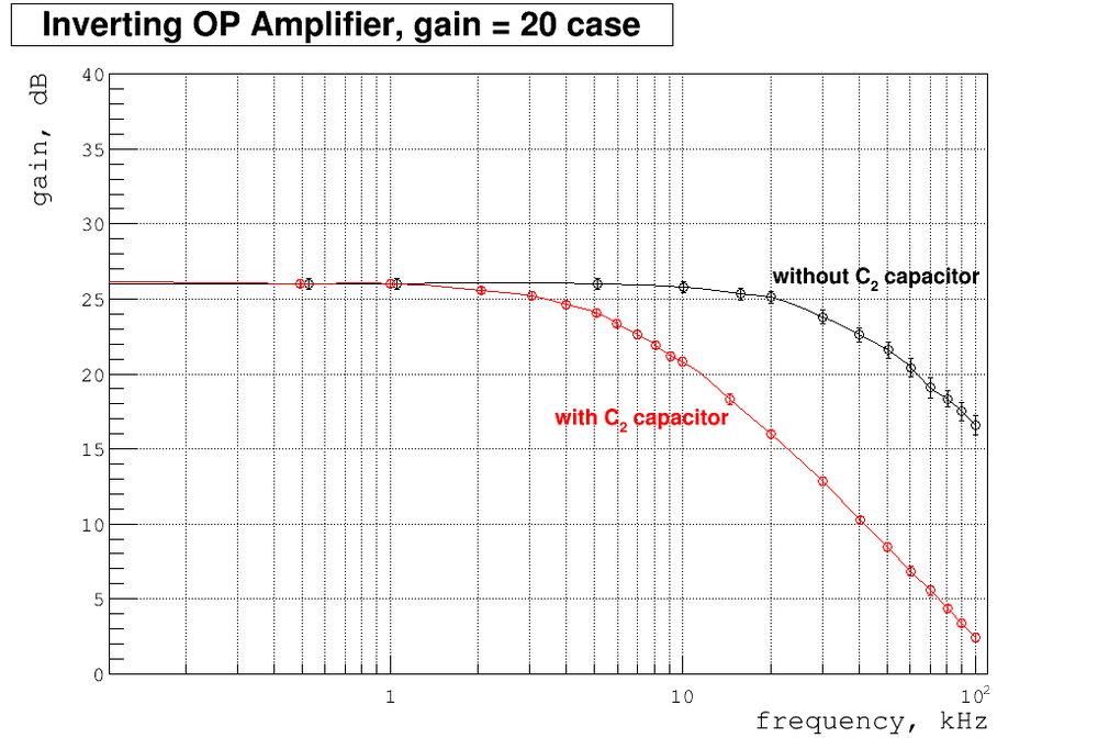
Below my plot of gain as function of frequency. Also I overplay here my previous measurements of gain without capacitor .
As we can see the gain are dropping down at about calculated above frequency. It's can be easily understood. At this point the capacitor starts to conduct AC signal reducing the effective resistors value. So at hight frequency the gain = starts to drop below the usual value without capacitor. It's sometimes very useful because by decreasing the gain at high frequencies we can prevent unwanted possible oscillations at this point ,
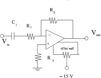
Capacitor in series with
1) Select a capacitor such that when = 1 kHz.
I will pick up:
(can compose like 10nF || (10nF + 10nF))
and my break point becomes:
2) Add the capacitor in series to so you have the circuit shown above.
3) Use a pulse generator to input a sinusoidal voltage
4) Measure the Gain as a function of the frequency and plot it.
Below my measurements and gain calculation:
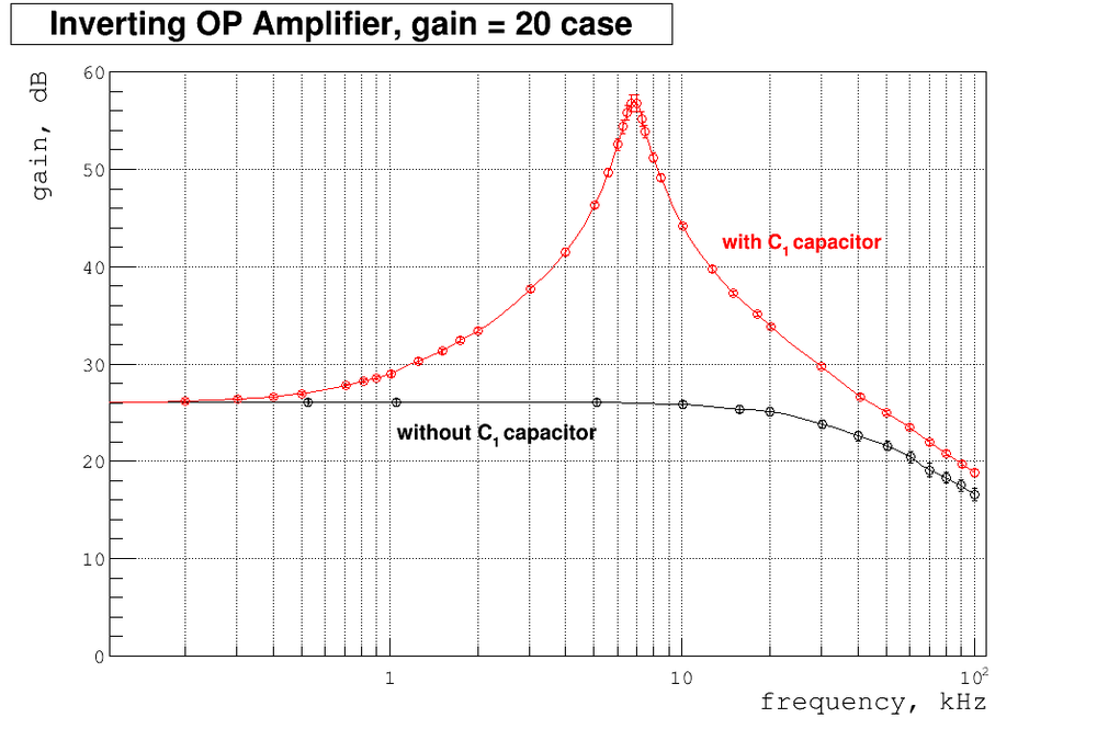
Below my plot of gain as function of frequency. Also I overplay here my previous measurements of gain without capacitor .
As we can see the gain starts to go up at about 1 kHz, reaches maximum at about 7 kHz and then goes down. It can be understood as follow. At break point frequency calculated above the capacitor starts to conduct the AC signal very well. So we are effectively reduce the resistor values and as follow increase the gain = . As frequency goes up the competing process of decreasing gain starts to work. And at some point the total gain starts to go down.
Slew rate
Measure the slew and compare it to the factory spec.
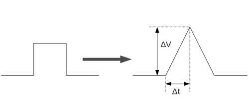
Below is the table with my measurements and calculated Slew Rate. I did these measurements for several high frequency points. My input signal was squared wave and I increased the input voltage until I observed the squared wave was transformed to triangle wave so I can measure the Slew Rate as the slope of line:
My best estimate for measured Slew Rate is:
From the data sheet the typical slew rate values for LM741 is:
.
Because it's the typical values and probably varies from one chip to other I think my measured values of slew rate is reasonable and in agreement with data sheet for this type of OP AMP
Power Supply Rejection Ratio
- Set = 0.
- Measure while changing
Below are my measurements of as function (and I used the and ):
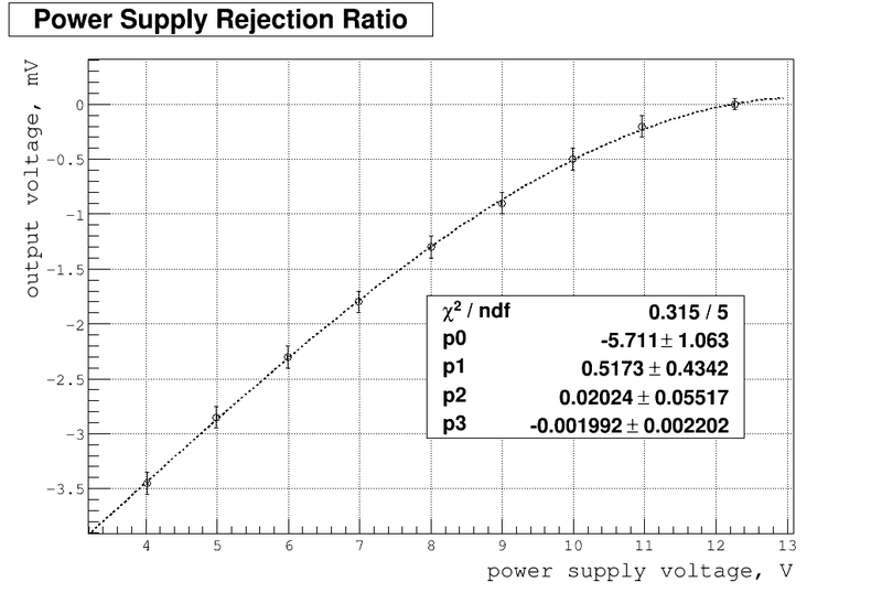
Below is my plot of as function :
The experimental points was approximated by polynomial as:
where
The power supply rejection ratio (PSRR) can be calculated by
Using the polynomial above
and substituting the corresponding coefficients and evaluating the PSRR at point (the data sheet values of PSRR is given at , but I can not really evaluate my PSRR at this point because my fitting procedure and my measured values are out of this point):
By doing math and handling the error propagation we get finally:
As we can see the calculated PSRR values is pretty close to data sheet typical values of -96 dB (at ). Unfortunately my error is too high. One way to handle it would be to improve the error of measured small quantities of output voltage. The other way would be to improve the method used to analyze the experimental points, especially find the better approximation function with smaller fitting errors. Also I really need the power supply able to give the varying voltage at about so I can make the corresponding comparison with data sheet value.
Output voltage RMS noise
My measured peak-to-peak noise with grounded is:
So my RMS noise is:
Go Back to All Lab Reports Forest_Electronic_Instrumentation_and_Measurement
