Difference between revisions of "Lab 9 RS"
| (63 intermediate revisions by the same user not shown) | |||
| Line 8: | Line 8: | ||
[[File:TF_EIM_Lab9.png | 400 px]] | [[File:TF_EIM_Lab9.png | 400 px]] | ||
| + | |||
| + | |||
| + | I am going to use: | ||
| + | |||
| + | 1) Zener diode 4.7 V 1N5230B-T | ||
| + | 2) the resistor <math>R = 10.3 \Omega</math> | ||
| + | |||
| + | |||
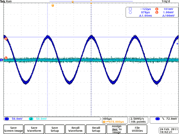
2.) Use a sine wave generator to drive the circuit so <math>V_{in} = V_0 \cos(2 \pi \nu t)</math> where <math>V_0 = 0.1</math> V and <math> \nu</math> = 1kHz. (20 pnts) | 2.) Use a sine wave generator to drive the circuit so <math>V_{in} = V_0 \cos(2 \pi \nu t)</math> where <math>V_0 = 0.1</math> V and <math> \nu</math> = 1kHz. (20 pnts) | ||
| Line 13: | Line 21: | ||
3.) Based on your observations using a oscilloscope, sketch the voltages <math>V_{in}</math> and <math>V_{out}</math> as a function of time. | 3.) Based on your observations using a oscilloscope, sketch the voltages <math>V_{in}</math> and <math>V_{out}</math> as a function of time. | ||
| − | [[File: | + | [[File:Tek00034.png | 600 px]] |
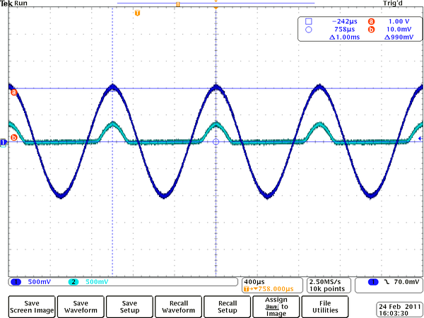
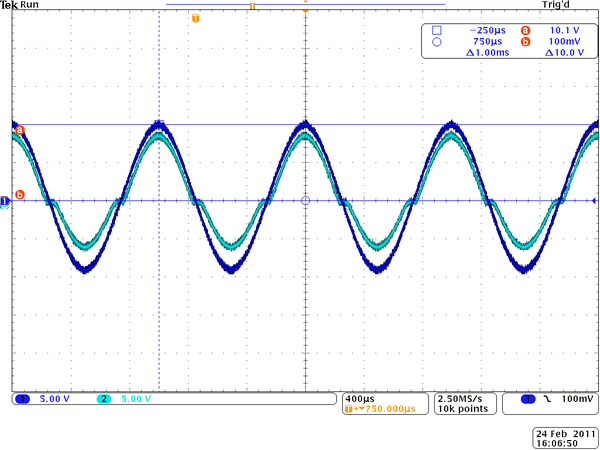
4.) Do another sketch for <math>V_0 </math> = 1.0 V and another for 10.0 V (DONT LET ANY SMOKE OUT!). (20 pnts) | 4.) Do another sketch for <math>V_0 </math> = 1.0 V and another for 10.0 V (DONT LET ANY SMOKE OUT!). (20 pnts) | ||
| − | |||
| + | Below my screen save for <math>V_0 </math> = 1.0 V | ||
| − | [[File: | + | [[File:Tek00035.png | 600 px]] |
| + | |||
| + | |||
| + | And below my screen save for <math>V_0 </math> = 10.0 V | ||
| + | |||
| + | [[File:Tek00036.png | 600 px]] | ||
| + | |||
| + | |||
| + | For the last sketch the output voltage is <math>V_{out} = 8.6\ V</math>. Let's estimate the power dissipated in resistor and diode. The current can be calculated by <math>I=\frac{V_{out}}{R}=\frac{8.6\ V}{10.3\ k\Omega} = 0.83\ mA</math>. | ||
| + | |||
| + | The resistor power is given by <math>P_R=I\cdot V_{out} = 0.83\ mA \cdot 8.6\ V = 7.14\ mW</math>. So we are OK here. | ||
| + | |||
| + | The diode power is given by <math>P_R=I\cdot V_{diode} = 0.83\ mA \cdot (10 - 8.6)\ V = 1.16\ mW</math>. So we are OK here as well. '''No any smoke out.''' | ||
= Differentiating Circuit with clipping= | = Differentiating Circuit with clipping= | ||
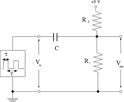
| Line 37: | Line 57: | ||
| − | Also because we want <math>V_{out} = 3\ V</math> and using <math>V_{out} = V_{in}\cdot\frac{R_2}{R_1+R_2}</math>. | + | Also because we want <math>V_{in} = 5\ V</math> and <math>V_{out} = 3\ V</math> without any input pulse and using <math>V_{out} = V_{in}\cdot\frac{R_2}{R_1+R_2}</math>. Solving this simple equation we get the second condition for <math>R_1</math> and <math>R_2</math> |
| + | |||
| + | <math>2)\ \ R_1 = 1.5\ R_2</math> | ||
| + | |||
| + | I am going to use <math>R_1 = 10\ k\Omega</math> and <math>R_2 = 15\ k\Omega</math> which satisfy both conditions above | ||
| + | |||
| + | |||
| − | + | 3) Select a capacitor <math>(C)</math> and a pulse width <math>\tau</math> to form a differentiating circuit for the pulse from the signal generator. Hint: <math>R_{12}C \ll \tau</math>. | |
| + | Taking <math>R_1=10.15\ k\Omega</math> and <math>R_2=14.90\ k\Omega \Rightarrow R_{12}=\frac{R_1 R_2}{(R_1+R_2)} = 6.04\ k\Omega</math>. Also taking <math>C = 9.65\ nF</math>. Now I can calculate the time constant of my <math>RC</math> circuit as <math>R_{12}C = 58.3\ us</math>. | ||
| − | + | ||
| + | By selecting the pulse width <math>\tau \approx 400.0\ ms \gg 58.3\ us</math> I will be able to make a good differentiator circuit. | ||
| + | 4) plot <math>V_{in}</math> and <math>V_{out}</math> as a function of time using your scope observations. (20 pnts) | ||
| − | |||
| + | Below the "screen save" of <math>V_{in}</math> and <math>V_{out}</math> as a function of time for the case <math>V_{in} = 1\ Volts</math> | ||
| + | |||
| + | [[File:Tek00040.png | 600 px]] | ||
| − | |||
| − | + | Now I changed the input voltage to <math>V_{in} = 3\ Volts</math>. As we can see from the plot below the output signal does change as well. | |
| + | [[File:Tek00041.png | 600 px]] | ||
| + | So there is no any clipping off the output signal for the circuit above. | ||
| − | |||
5) Now add the diode circuit from part 1 to prevent <math>V_{out}</math> from rising above +5 V. Sketch the new circuit below. | 5) Now add the diode circuit from part 1 to prevent <math>V_{out}</math> from rising above +5 V. Sketch the new circuit below. | ||
| + | |||
| + | [[File:Cuircuit 2.png | 400 px]] | ||
6) plot <math>V_{in}</math> and <math>V_{out}</math> as a function of time with the diode circuit you added using your scope observations. (the diode should clip off positive spikes) (20 pnts) | 6) plot <math>V_{in}</math> and <math>V_{out}</math> as a function of time with the diode circuit you added using your scope observations. (the diode should clip off positive spikes) (20 pnts) | ||
| + | |||
| + | |||
| + | Below the "screen save" of <math>V_{in}</math> and <math>V_{out}</math> as a function of time for the case <math>V_{in} = 1\ Volts</math> | ||
| + | |||
| + | [[File:Tek00042.png | 800 px]] | ||
| + | |||
| + | |||
| + | Now I changed the input voltage to <math>V_{in} = 3\ Volts</math>. As we can see from the plot below the output signal doesn't change at all. | ||
| + | |||
| + | [[File:Tek00043.png | 800 px]] | ||
| + | |||
| + | |||
| + | Now my diode is clipping off the positive signal at about +5 V and is clipping off the negative signal at about -1 V. | ||
| + | And the output signal doesn't change when we change the amplitude of input signal. | ||
=Questions= | =Questions= | ||
#Explain your results in parts 1 & 2 in terms of the diode turn-on voltage. (20 pnts) | #Explain your results in parts 1 & 2 in terms of the diode turn-on voltage. (20 pnts) | ||
| + | |||
| + | All explanation is based on current voltage diagram for diode used in this laboratory work. I used the ZENER silicon diode type # 1N5230B-T. The diode current vs. diode voltage plot I measured in previous lab (see my pictures below): | ||
| + | |||
| + | [[File:L8 diod current m1.png | 400 px]] | ||
| + | |||
| + | The critical parameters here is '''reverse turn on voltage''' and '''forward turn on voltage'''. Reverse turn on voltage for this type of diode equal about 4.7 Volts and forward turn on voltage about 0.9 Volts. When the voltage drop on diode is beyond this two points the diode becomes good conductor with internal resistance about 4-6 <math>\Omega</math>. On the other side when voltage below 0.8 Volts in forward direction or below 4.7 Volts in reverse direction the diode becomes good insulator with current less than 1 mA through the diode. All explanation of the clipping current can be done by using the voltage current diagram above and by using reverse and forward turn on voltage points. | ||
| + | |||
| + | 1) Let see what happens for the first clipping circuit: | ||
| + | |||
| + | [[File:TF_EIM_Lab9.png | 300 px]] | ||
| + | |||
| + | a) When the input voltage is about 0.1 Volts the diode is below the reverse and forward turn on voltage points. The diode is working as a good insulator and there are no any signal at output because all voltage drop is on the diode. | ||
| + | |||
| + | b) When the input voltage is about 1 Volts we are above the forward turn on voltage. So the diode becomes to conduct in forward direction when the voltage drop on diode exceed 0.8 Volts. All input signal that above 0.8 Volts is going through the diode. On the other side we are still bellow 4.7 Volts on the negative side of input signal. So the diode cut all negative signal off. | ||
| + | |||
| + | c) When the input voltage is about 10 Volts we are above the forward turn on voltage and we are above the reverse turn on voltage as well. So diode becomes to conduct and all input signal that exceed 0.8 Volts in forward direction and that exceed 4.7 Volts in reverse direction is going through the diode so we can see the output signal. | ||
| + | |||
| + | |||
| + | 1) Let see what happens for the second clipping circuit: | ||
| + | |||
| + | [[File:cuircuit_2.png | 300 px]] | ||
| + | |||
| + | Here we shut off the output resistor by diode. So when the output signal through the diode exceeds 0.8 Volts in forward direction and 4.7 Volts in reverse direction the diode becomes to conduct and all output signal is going through the diode to ground. Also note that diode here is actually in forward direction with respect to ground. So the diode is going to cut off all positive signal that exceed 4.7 Volts and cut off all negative signal that exceed 0.8 Volts. | ||
Latest revision as of 20:15, 1 March 2011
Lab 9: Diode Circuits
Clipping Circuit
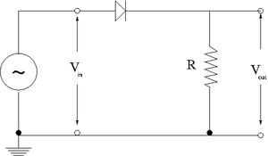
1.) Construct the circuit shown below using a silicon diode.
I am going to use:
1) Zener diode 4.7 V 1N5230B-T
2) the resistor
2.) Use a sine wave generator to drive the circuit so where V and = 1kHz. (20 pnts)
3.) Based on your observations using a oscilloscope, sketch the voltages and as a function of time.
4.) Do another sketch for = 1.0 V and another for 10.0 V (DONT LET ANY SMOKE OUT!). (20 pnts)
Below my screen save for = 1.0 V
And below my screen save for = 10.0 V
For the last sketch the output voltage is . Let's estimate the power dissipated in resistor and diode. The current can be calculated by .
The resistor power is given by . So we are OK here.
The diode power is given by . So we are OK here as well. No any smoke out.
Differentiating Circuit with clipping
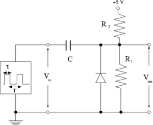
1) Construct the circuit below.
2) Select and such that the current from the +5V DC source is less than 1.0 mA and the DC voltage at is 3 V when there is no input pulse.
Because we want to keep the current below and using . Solving this inequality we get the first condition for and
Also because we want and without any input pulse and using . Solving this simple equation we get the second condition for and
I am going to use and which satisfy both conditions above
3) Select a capacitor and a pulse width to form a differentiating circuit for the pulse from the signal generator. Hint: .
Taking and . Also taking . Now I can calculate the time constant of my circuit as .
By selecting the pulse width I will be able to make a good differentiator circuit.
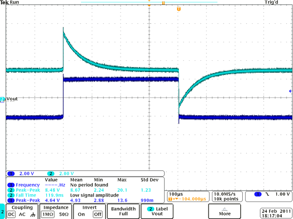
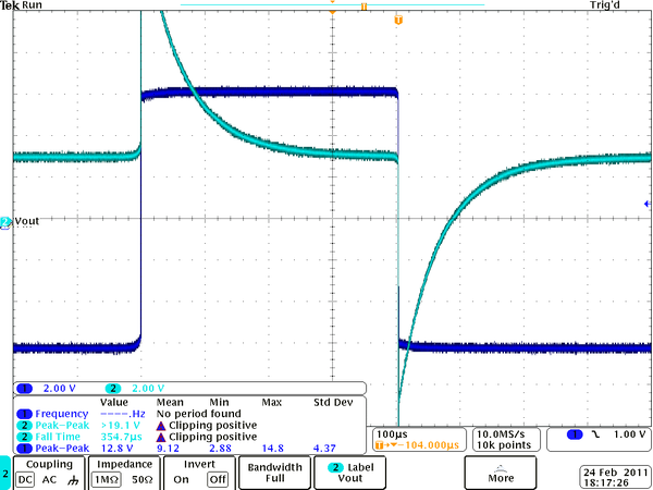
4) plot and as a function of time using your scope observations. (20 pnts)
Below the "screen save" of and as a function of time for the case
Now I changed the input voltage to . As we can see from the plot below the output signal does change as well.
So there is no any clipping off the output signal for the circuit above.
5) Now add the diode circuit from part 1 to prevent from rising above +5 V. Sketch the new circuit below.
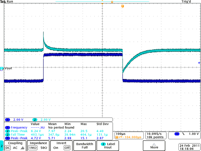
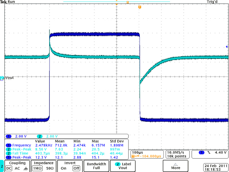
6) plot and as a function of time with the diode circuit you added using your scope observations. (the diode should clip off positive spikes) (20 pnts)
Below the "screen save" of and as a function of time for the case
Now I changed the input voltage to . As we can see from the plot below the output signal doesn't change at all.
Now my diode is clipping off the positive signal at about +5 V and is clipping off the negative signal at about -1 V.
And the output signal doesn't change when  we  change the amplitude of input signal.
Questions
- Explain your results in parts 1 & 2 in terms of the diode turn-on voltage. (20 pnts)
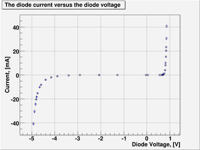
All explanation is based on current voltage diagram for diode used in this laboratory work. I used the ZENER silicon diode type # 1N5230B-T. The diode current vs. diode voltage plot I measured in previous lab (see my pictures below):
The critical parameters here is reverse turn on voltage and forward turn on voltage. Reverse turn on voltage for this type of diode equal about 4.7 Volts and forward turn on voltage about 0.9 Volts. When the voltage drop on diode is beyond this two points the diode becomes good conductor with internal resistance about 4-6 . On the other side when voltage below 0.8 Volts in forward direction or below 4.7 Volts in reverse direction the diode becomes good insulator with current less than 1 mA through the diode. All explanation of the clipping current can be done by using the voltage current diagram above and by using reverse and forward turn on voltage points.
1) Let see what happens for the first clipping circuit:
a) When the input voltage is about 0.1 Volts the diode is below the reverse and forward turn on voltage points. The diode is working as a good insulator and there are no any signal at output because all voltage drop is on the diode.
b) When the input voltage is about 1 Volts we are above the forward turn on voltage. So the diode becomes to conduct in forward direction when the voltage drop on diode exceed 0.8 Volts. All input signal that above 0.8 Volts is going through the diode. On the other side we are still bellow 4.7 Volts on the negative side of input signal. So the diode cut all negative signal off.
c) When the input voltage is about 10 Volts we are above the forward turn on voltage and we are above the reverse turn on voltage as well. So diode becomes to conduct and all input signal that exceed 0.8 Volts in forward direction and that exceed 4.7 Volts in reverse direction is going through the diode so we can see the output signal.
1) Let see what happens for the second clipping circuit:
Here we shut off the output resistor by diode. So when the output signal through the diode exceeds 0.8 Volts in forward direction and 4.7 Volts in reverse direction the diode becomes to conduct and all output signal is going through the diode to ground. Also note that diode here is actually in forward direction with respect to ground. So the diode is going to cut off all positive signal that exceed 4.7 Volts and cut off all negative signal that exceed 0.8 Volts.
Forest_Electronic_Instrumentation_and_Measurement Go Back to All Lab Reports

