Difference between revisions of "Lab 17 RS"
| (14 intermediate revisions by the same user not shown) | |||
| Line 24: | Line 24: | ||
| Zero-Gate-Voltage Drain Current ||<math> I_{DSS}</math> || 2.0 || 20 || mAdc | | Zero-Gate-Voltage Drain Current ||<math> I_{DSS}</math> || 2.0 || 20 || mAdc | ||
|- | |- | ||
| − | | Gate-Source Cutoff Voltage|| <math>V_{GS(off)}</math> || - || -8.0 || Vdc | + | | Gate-Source Cutoff Voltage || <math>V_{GS(off)}</math> || - || -8.0 || Vdc |
|- | |- | ||
| − | | Total Device Dissipation @ <math>T_A=25^oC</math> | + | | Total Device Dissipation @ <math>T_A=25^oC</math> |
| + | | <math>P_{max}</math> | ||
| + | | colspan="2" | 350 | ||
| + | | mW | ||
|- | |- | ||
| − | |Gait resistor | + | | Gait resistor |
| − | | <math> | + | | <math>R_G</math> |
| colspan="2" | 3.3 | | colspan="2" | 3.3 | ||
| M<math>\Omega</math> | | M<math>\Omega</math> | ||
|- | |- | ||
| − | |Drain resistor | + | | Drain resistor |
| <math>R_D</math> | | <math>R_D</math> | ||
| − | |colspan="2" | 1.0 | + | | colspan="2" | 1.0 |
| k<math>\Omega</math> | | k<math>\Omega</math> | ||
|- | |- | ||
| − | | ||<math>y_{fs}</math> || | + | | Forward Transfer Admittance || <math>y_{fs}</math> || 2000 || 7500 || <math>\mu</math>mhos |
| − | | | ||
| − | | ||<math> | ||
|- | |- | ||
| − | | ||<math>y_{ | + | | Input Admittance || <math>y_{is}</math> || - || 800 || <math>\mu</math>mhos |
|- | |- | ||
| + | | Output Conductance || <math>y_{os}</math> || - || 200 || <math>\mu</math>mhos | ||
|} | |} | ||
| Line 66: | Line 68: | ||
| − | [[File:Table01.png | | + | [[File:Table01.png | 550 px]] |
| − | [[File:Table02.png | | + | [[File:Table02.png | 550 px]] |
| − | [[File:Table03.png | | + | [[File:Table03.png | 550 px]] |
| − | [[File:Table04.png | | + | [[File:Table04.png | 550 px]] |
| Line 78: | Line 80: | ||
| − | [[File:L17 id vs vgs.png | | + | [[File:L17 id vs vgs.png | 800 px]] |
| − | |||
| − | |||
=4.) Plot <math> I_D</math> -vs- <math>V_{GS}</math> (30 pnts)= | =4.) Plot <math> I_D</math> -vs- <math>V_{GS}</math> (30 pnts)= | ||
| Line 93: | Line 93: | ||
| − | [[File:L17 id vs vgs 21.png | | + | [[File:L17 id vs vgs 21.png | 800 px]] |
Latest revision as of 16:41, 13 April 2011
The JFET (Junction Field Effect Transistor n-channel)
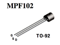
File:JFET MPF102 DataSheet.pdf
1). Complete the table below for the JFET.
| Characteristic | Symbol | Min | Max | Unit |
|---|---|---|---|---|
| Zero-Gate-Voltage Drain Current | 2.0 | 20 | mAdc | |
| Gate-Source Cutoff Voltage | - | -8.0 | Vdc | |
| Total Device Dissipation @ | 350 | mW | ||
| Gait resistor | 3.3 | M | ||
| Drain resistor | 1.0 | k | ||
| Forward Transfer Admittance | 2000 | 7500 | mhos | |
| Input Admittance | - | 800 | mhos | |
| Output Conductance | - | 200 | mhos | |
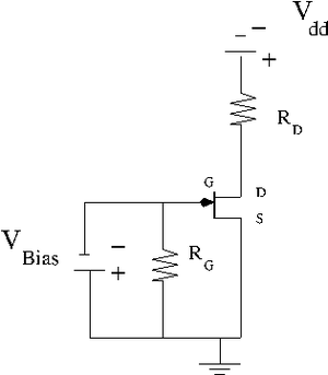
2.) Construct the JFET circuit below.
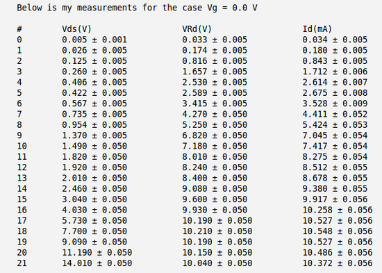
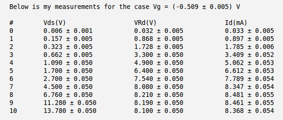
3.) Plot measurements of -vs- by varying for = 0, 0.5, 1.0, 1.5 V. (40 pnts)
I have used the following resistors:
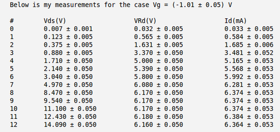
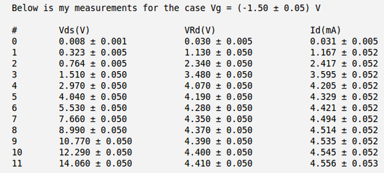
Below is the table with my measurements of voltages and and calculation of the current . Here I have used the meter to measure directly the voltage drop between the drain and source and to measure the voltage drop on resistor .
So my calculated current becomes:
.
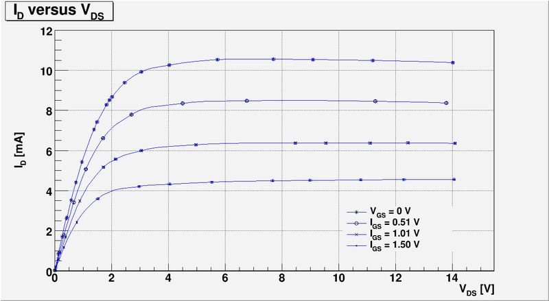
And below I have plotted four curves as function of for four different values of
4.) Plot -vs- (30 pnts)
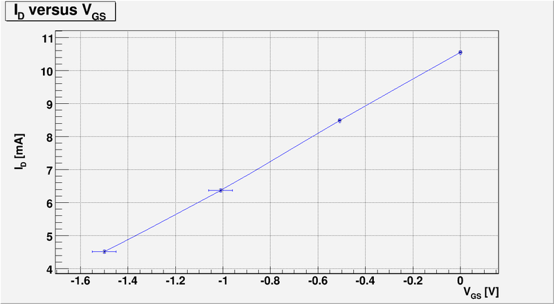
For every measured values I have picked up the current values in the middle of saturation region of each line as follow:
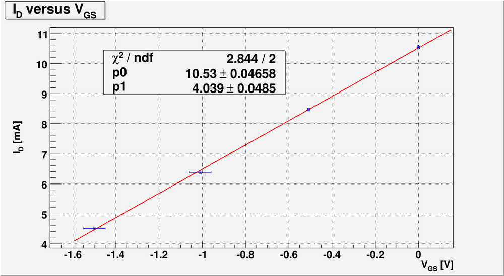
And below is my plot of -vs- :
5.) Calculate for your JFET (20 pnts)
For common source configuration JFET:
So to calculate we need to know the functional dependence of . Lets approximate this function by line using my measurements and plot above:
The line equation is:
Also note that this line equation was obtained using about the same voltage in saturation region from my first measurements of as function of for four different values of . So we can take the partial derivative of with respect to using the line equation above. Finally,
Question
Does depend on ? (10 pnts)
No. As we can see from calculation above is constant and does not depend from . That is true if we are working in saturation region where the functional dependence of with respect to is line so
If we are in active region of as function of the functional form of with respect to is not the line anymore and will depend on .
Go Back to All Lab Reports Forest_Electronic_Instrumentation_and_Measurement
