Difference between revisions of "Lab 14 RS"
| Line 23: | Line 23: | ||
The load line equation becomes: | The load line equation becomes: | ||
| − | <math>I_C = \frac{V_{CC}-V_{CE}}{R_E+R_C} = \frac{(11 - V_{CE}\ V}{2.2\ k\Omega} </math> | + | <math>I_C = \frac{V_{CC}-V_{CE}}{R_E+R_C} = \frac{(11 - V_{CE})\ V}{2.2\ k\Omega} </math> |
==Draw a load line using the <math>I_{C}</math> -vs- <math>I_{EC}</math> from the previous lab 13. Record the value of <math>h_{FE}</math> or <math>\beta</math>.== | ==Draw a load line using the <math>I_{C}</math> -vs- <math>I_{EC}</math> from the previous lab 13. Record the value of <math>h_{FE}</math> or <math>\beta</math>.== | ||
Revision as of 20:30, 21 March 2011
The Common Emitter Amplifier
Circuit
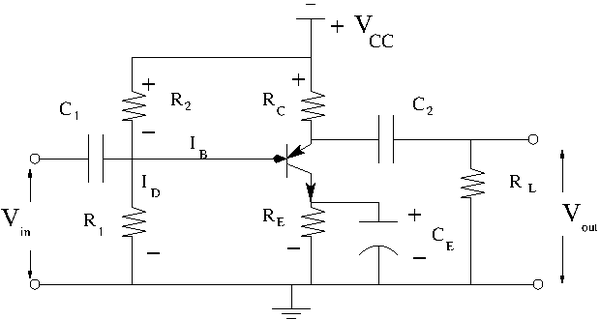
Construct the common emitter amplifier circuit below according to your type of emitter.
Calculate all the R and C values to use in the circuit such that
- a. Try and
- b. mA DC with no input signal
- c. V
- d. to prevent burnout
- e.
- f. mA
Let's , and .
The load line equation becomes:
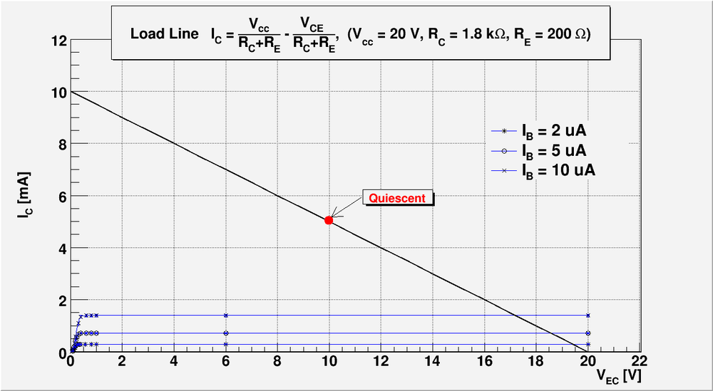
Draw a load line using the -vs- from the previous lab 13. Record the value of or .
On the plot above I overlay me output lines from the previous lab report #13 and the load line I am going to use to construct amplifier.
My based on my previous lab report #13
Set a DC operating point so it will amplify the input pulse given to you. Some of you will have sinusoidal pulses others will have positive or negative only pulses.
I will set up my operating point in the middle of the load line: , .
Let's calculate all bias voltage to set up this operating point.
To set up the operating point above we need to set up .
We have:
.
Here are have used instead of because it's my actual values here.
To get operating point independent of the transistor base current we want
Let's
So
And we can find from Kirchhoff voltage Low:
. Here
So
Measure all DC voltages in the circuit and compare with the predicted values.(10 pnts)
My predicted DC voltage are:
We have from operating point:
And because we have silicon transistor:
Now
My measured DC voltage are:
First note that my is close to predicted values .
Also note that my is a little higher than my initial operating point . The main reason is that my actual values of instead of as I was assumed initially. That will reduce my voltage that reduce my current. So I will shift to right my operating point from to lower values and correspondingly will increase my .
By direct measurements my operating point now is and
Let's check do my operating point is still on my load line. I have , . So from load line equation:
.
So my operating point lies in my load line within experimental error.
Measure the voltage gain as a function of frequency and compare to the theoretical value.(10 pnts)
Measure and at about 1 kHz and compare to the theoretical value.(10 pnts)
How do you do this? Add resistor in front of which you vary to determine and then do a similar thing for except the variable reistor goes from to ground.
Measure and as a function of frequency with removed.(10 pnts)
Questions
- Why does a flat load line produce a high voltage gain and a steep load line a high current gain? (10 pnts)
- What would be a good operating point an an common emitter amplifier used to amplify negative pulses?(10 pnts)
- What will the values of , , and be if the transistor burns out resulting in infinite resistance. Check with measurement.(10 pnts)
- What will the values of , , and be if the transistor burns out resulting in near ZERO resistance (ie short). Check with measurement.(10 pnts)
- Predict the change in the value of if is increased from 10 to 50 (10 pnts)
- Sketch the AC equivalent circuit of the common emitter amplifier.(10 pnts)
Go Back to All Lab Reports Forest_Electronic_Instrumentation_and_Measurement

