Difference between revisions of "Lab 13 RS"
| Line 14: | Line 14: | ||
=Transistor circuit= | =Transistor circuit= | ||
| − | + | == Identify the type (n-p-n or p-n-p) of transistor you are using and fill in the following specifications. == | |
| Line 50: | Line 50: | ||
| − | + | == Construct the circuit below according to the type of transistor you have. == | |
[[File:TF_EIM_Lab13a_Circuit.png | 300 px]][[File:TF_EIM_Lab13_Circuit.png | 300 px]] | [[File:TF_EIM_Lab13a_Circuit.png | 300 px]][[File:TF_EIM_Lab13_Circuit.png | 300 px]] | ||
| Line 74: | Line 74: | ||
| − | + | == Measure the emitter current <math>I_E</math> for several values of <math>V_{CE}</math> by changing <math>V_{CC}</math> such that the base current <math>I_B = 2 \mu</math> A is constant. <math>I_B \approx \frac{V_{BB}-V_{BE}}{R_B}</math> == | |
| − | {| border="1" | + | {| border="1" cellspacing="0" cellpadding="10" style="text-align: center" |
| − | + | !scope="row" |<math>V_{CC}</math> | |
| − | |V_{CC} || | + | !scope="row" |<math>V_{B}</math> |
| − | |- | + | !scope="row" |<math>V_{BB}</math> |
| + | !scope="row" |<math>V_{EC}</math> | ||
| + | !scope="row" |<math>V_{E}</math> | ||
| + | !scope="row" |<math>R_{E}</math> | ||
| + | !scope="row" |<math>R_{B}</math> | ||
| + | !scope="row" |<math>I_{E}</math> | ||
| + | !scope="row" |<math>I_{B}</math> | ||
| + | |- | ||
|mV || mV || V || mV || mV || <math>\Omega</math> || k<math>\Omega</math>|| mA|| \muA | |mV || mV || V || mV || mV || <math>\Omega</math> || k<math>\Omega</math>|| mA|| \muA | ||
|- | |- | ||
| Line 90: | Line 97: | ||
| − | + | == Repeat the previous measurements for <math>I_B \approx 5 \mbox{ and } 10 \mu</math> A. Remember to keep <math>I_CV_{CE} < P_{max}</math> so the transistor doesn't burn out | |
| − | {| border="1" |cellpadding="20" cellspacing="0 | + | {| border="1" |cellpadding="20" cellspacing="0 == |
|- | |- | ||
|V_{CC} || V_B || V_{BB} || V_ {EC} || V_ E || R_E || R_B || I_E || I_B | |V_{CC} || V_B || V_{BB} || V_ {EC} || V_ E || R_E || R_B || I_E || I_B | ||
Revision as of 04:43, 11 March 2011
DC Bipolar Transistor Curves
Data sheet for transistors.
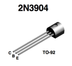
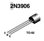
Media:2N3904.pdfMedia:2N3906.pdf
Using 2N3904 is more srtaight forward in this lab.
Transistor circuit
Identify the type (n-p-n or p-n-p) of transistor you are using and fill in the following specifications.
I am going to use n-p-n transistor 2N3904. Below are some specifications from data shits for this type of transistor:
| Value | Description | ||
|---|---|---|---|
| Collector-Base breakdown voltage | |||
| Emitter-Base Breakdown Voltage | |||
| Maximum Collector-Emitter Voltage | |||
| Maximum Collector-Emitter Voltage | |||
| Maximum Collector Current - Continuous | |||
| Transistor Power rating() | |||
| , | |||
| 40 | 300 | , | |
| 70 | 300 | , | |
| 100 | 300 | , | |
| 60 | 300 | , | |
| 30 | 300 | , | |
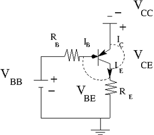
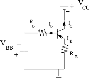
Construct the circuit below according to the type of transistor you have.
Let .
variable power supply
.
Find the resistors you need to have
, , and
By measurements I was able to find that . So I am going to use this value. Also let picks up . So my current .
Now to get I need to use To get I need to use To get I need to use
Measure the emitter current for several values of by changing such that the base current A is constant.
| mV | mV | V | mV | mV | k | mA | \muA | |
== Repeat the previous measurements for A. Remember to keep so the transistor doesn't burn out
| V_{CC} | V_B | V_{BB} | V_ {EC} | V_ E | R_E | R_B | I_E | I_B |
| mV | mV | V | mV | mV | k | mA | \muA | |
5.) Graph -vs- for each value of and above. (40 pnts)
6.) Overlay points from the transistor's data sheet on the graph in part 5.).(10 pnts)
Questions
- Compare your measured value of or for the transistor to the spec sheet? (10 pnts)
- What is for the transistor?(10 pnts)
- The base must always be more _________(________) than the emitter for a npn (pnp)transistor to conduct I_C.(10 pnts)
- For a transistor to conduct I_C the base-emitter junction must be ___________ biased.(10 pnts)
- For a transistor to conduct I_C the collector-base junction must be ___________ biased.(10 pnts)
Extra credit
Measure the Base-Emmiter breakdown voltage. (10 pnts)
I expect to see a graph and a linear fit which is similar to the forward biased diode curves. Compare your result to what is reported in the data sheet.
Go Back to All Lab Reports Forest_Electronic_Instrumentation_and_Measurement


