Difference between revisions of "Lab 13 TF EIM"
| (26 intermediate revisions by 2 users not shown) | |||
| Line 1: | Line 1: | ||
| − | DC Transistor Curves | + | DC Bipolar Transistor Curves |
| + | |||
| + | Data sheet for transistors. | ||
| + | |||
| + | [[Media:2N3904.pdf]][[Media:2N3906.pdf]] | ||
| + | |||
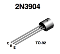
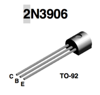
| + | [[File:2N3904_PinOuts.png | 200 px]][[File:2N3906_PinOuts.png | 200 px]] | ||
| + | |||
| + | |||
| + | Using 2N3904 is more srtaight forward in this lab. | ||
=Transistor circuit= | =Transistor circuit= | ||
| − | + | 1.) Identify the type (n-p-n or p-n-p) of transistor you are using and fill in the following specifications. | |
| − | + | ||
| − | + | ||
| − | + | {| border="1" |cellpadding="20" cellspacing="0 | |
| − | + | |- | |
| − | + | |Value || Description | |
| + | |- | ||
| + | | || Collector-Base breakdown voltage | ||
| + | |- | ||
| + | | || Emitter-Base Breakdown Voltage | ||
| + | |- | ||
| + | | || Maximum Collector Voltage | ||
| + | |- | ||
| + | | || Maximum Collector Current | ||
| + | |- | ||
| + | | || Transistor Power rating(<math>P_{Max}</math>) | ||
| + | |- | ||
| + | | || DC current gain <math>h_{FE}( I_C, V_{CE})</math> | ||
| + | |} | ||
| + | |||
| + | |||
| + | |||
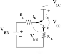
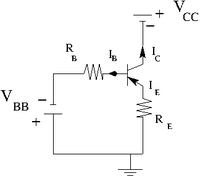
| + | 2.) Construct the circuit below according to the type of transistor you have. | ||
| + | |||
| + | [[File:TF_EIM_Lab13a_Circuit.png | 200 px]][[File:TF_EIM_Lab13_Circuit.png | 200 px]] | ||
| + | |||
| + | |||
| + | Let <math>R_E = 100 \Omega</math>. | ||
| + | |||
| + | <math>V_{CC} < 5 Volts</math> variable power supply | ||
| + | |||
| + | <math>V_{BE}= 1V</math>. | ||
| + | |||
| + | Find the resistors you need to have | ||
| + | |||
| + | <math>I_B = 2 \mu A</math> , <math>5 \mu A</math> , and <math>10 \mu A</math> | ||
| + | |||
| + | 3.) Measure the emitter current <math>I_E</math> for several values of <math>V_{CE}</math> by changing <math>V_{CC}</math> such that the base current <math>I_B = 2 \mu</math> A is constant. <math>I_B \approx \frac{V_{BB}-V_{BE}}{R_B}</math> | ||
| + | |||
| + | |||
| + | |||
| + | {| border="1" |cellpadding="20" cellspacing="0 | ||
| + | |- | ||
| + | |V_{CC} || V_B || V_{BB} || V_ {EC} || V_ E || R_E || R_B || I_E || I_B | ||
| + | |- | ||
| + | |mV || mV || V || mV || mV || <math>\Omega</math> || k<math>\Omega</math>|| mA|| \muA | ||
| + | |- | ||
| + | | || || || || || || || || | ||
| + | |||
| + | |} | ||
| + | |||
| + | |||
| + | |||
| + | 4.) Repeat the previous measurements for <math>I_B \approx 5 \mbox{ and } 10 \mu</math> A. Remember to keep <math>I_CV_{CE} < P_{max}</math> so the transistor doesn't burn out | ||
| + | |||
| + | {| border="1" |cellpadding="20" cellspacing="0 | ||
| + | |- | ||
| + | |V_{CC} || V_B || V_{BB} || V_ {EC} || V_ E || R_E || R_B || I_E || I_B | ||
| + | |- | ||
| + | |mV || mV || V || mV || mV || <math>\Omega</math> || k<math>\Omega</math>|| mA|| \muA | ||
| + | |- | ||
| + | | || || || || || || || || | ||
| + | |||
| + | |} | ||
| + | |||
| + | |||
| + | |||
| + | 5.) Graph <math>I_C</math> -vs- <math>V_{CE}</math> for each value of <math>I_B</math> and <math>V_{CC}</math> above. (40 pnts) | ||
| + | |||
| + | 6.) Overlay points from the transistor's data sheet on the graph in part 5.).(10 pnts) | ||
=Questions= | =Questions= | ||
| − | # | + | #Compare your measured value of <math>h_{FE}</math> or <math>\beta</math> for the transistor to the spec sheet? (10 pnts) |
| − | #What is <math>\alpha</math> for the transistor? | + | #What is <math>\alpha</math> for the transistor?(10 pnts) |
| − | #The base must always be more _________(________) than the emitter for a npn (pnp)transistor to conduct I_C. | + | #The base must always be more _________(________) than the emitter for a npn (pnp)transistor to conduct I_C.(10 pnts) |
| − | #For a transistor to conduct I_C the base-emitter junction must be ___________ biased. | + | #For a transistor to conduct I_C the base-emitter junction must be ___________ biased.(10 pnts) |
| − | #For a transistor to conduct I_C the collector-base junction must be ___________ biased. | + | #For a transistor to conduct I_C the collector-base junction must be ___________ biased.(10 pnts) |
| + | |||
| + | =Extra credit= | ||
| + | |||
| + | Measure the Base-Emmiter breakdown voltage. (10 pnts) | ||
| + | I expect to see a graph <math>(I_{B} -vs- V_{BE} )</math> and a linear fit which is similar to the forward biased diode curves. Compare your result to what is reported in the data sheet. | ||
[[Forest_Electronic_Instrumentation_and_Measurement]] | [[Forest_Electronic_Instrumentation_and_Measurement]] | ||
Latest revision as of 04:03, 9 March 2011
DC Bipolar Transistor Curves
Data sheet for transistors.
Media:2N3904.pdfMedia:2N3906.pdf
Using 2N3904 is more srtaight forward in this lab.
Transistor circuit
1.) Identify the type (n-p-n or p-n-p) of transistor you are using and fill in the following specifications.
| Value | Description |
| Collector-Base breakdown voltage | |
| Emitter-Base Breakdown Voltage | |
| Maximum Collector Voltage | |
| Maximum Collector Current | |
| Transistor Power rating() | |
| DC current gain |
2.) Construct the circuit below according to the type of transistor you have.
Let .
variable power supply
.
Find the resistors you need to have
, , and
3.) Measure the emitter current for several values of by changing such that the base current A is constant.
| V_{CC} | V_B | V_{BB} | V_ {EC} | V_ E | R_E | R_B | I_E | I_B |
| mV | mV | V | mV | mV | k | mA | \muA | |
4.) Repeat the previous measurements for A. Remember to keep so the transistor doesn't burn out
| V_{CC} | V_B | V_{BB} | V_ {EC} | V_ E | R_E | R_B | I_E | I_B |
| mV | mV | V | mV | mV | k | mA | \muA | |
5.) Graph -vs- for each value of and above. (40 pnts)
6.) Overlay points from the transistor's data sheet on the graph in part 5.).(10 pnts)
Questions
- Compare your measured value of or for the transistor to the spec sheet? (10 pnts)
- What is for the transistor?(10 pnts)
- The base must always be more _________(________) than the emitter for a npn (pnp)transistor to conduct I_C.(10 pnts)
- For a transistor to conduct I_C the base-emitter junction must be ___________ biased.(10 pnts)
- For a transistor to conduct I_C the collector-base junction must be ___________ biased.(10 pnts)
Extra credit
Measure the Base-Emmiter breakdown voltage. (10 pnts)
I expect to see a graph and a linear fit which is similar to the forward biased diode curves. Compare your result to what is reported in the data sheet.


