Difference between revisions of "TF EIM Chapt3"
| Line 19: | Line 19: | ||
|- | |- | ||
|} | |} | ||
| + | |||
| + | The above images are suppose to represent the distribution of electrons in the crystal lattice cell. | ||
| + | |||
| + | |||
| + | To understand this structure more let's consider the structure of a 1-D crystal of atoms | ||
| + | |||
| + | |||
| + | A single free atom will have electrons bound to the atom due to the coulomb force. The bound electrons are found in various energy levels. | ||
| + | |||
| + | |||
| + | |||
| + | |||
There are 14 different Bravais lattice configurations | There are 14 different Bravais lattice configurations | ||
Revision as of 04:59, 15 February 2011
Semiconductor physics
There are 5 states of matter: Solid, liquid, gas, plasma (ionized gas) , and a Bose-Einstein condensate (quantum effects on a macroscopic scale).
Crystal Lattice
Semiconductor physics focuses on the solid state of matter in the form of crystals.
Crystals are formed when atoms are arranged in repeating structures called the crystal lattice. The recurrent structure which forms the crystal lattice is referred to a a cell.
Some popular cell names are
 |
 |

|
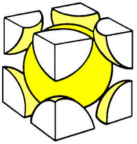
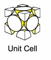
| (SC) Simple Cubic | (BCC) Body Centered Cubic | (FCC) Face Centered Cubic |
The above images are suppose to represent the distribution of electrons in the crystal lattice cell.
To understand this structure more let's consider the structure of a 1-D crystal of atoms
A single free atom will have electrons bound to the atom due to the coulomb force. The bound electrons are found in various energy levels.
There are 14 different Bravais lattice configurations
| Crystal System | Lattice type |
| Cubic | Simple, Face Centered, Body Centered |
| Tetragonal | Simple, Body Centered |
| Orthorhombic | Simple, Face Centered, Body Centered, End Centered |
| Monoclinic | Simple, End Centered |
| Rhombohedral | Simple |
| Triclinic | Simple |
| Hexagonal | Simple |
Most Semiconductors are made from Silicon and GaAs.
Silicon is a Face Centered Cubic cell
Silicon is an insulator if in pure form with 4 weakly bound (valence) electrons.
If you replace silicon atoms in the lattice with atoms that have either 3 valance or 5 valence electrons (doping) your can create sites with either a deficient number of electrons (a missing bond) or extra electrons (complete bond with a free electron)
By Doping silicon you can create sites with extra electrons (n-type) or sites with a deficient number of electrons (vacancies or holes ) (P-type)