Difference between revisions of "Lab 3 RS"
| (33 intermediate revisions by the same user not shown) | |||
| Line 19: | Line 19: | ||
2. Now construct the circuit using a non-polar capacitor | 2. Now construct the circuit using a non-polar capacitor | ||
| − | |||
| − | |||
3. Use a sinusoidal variable frequency oscillator to provide an input voltage to your filter | 3. Use a sinusoidal variable frequency oscillator to provide an input voltage to your filter | ||
| Line 26: | Line 24: | ||
4. Measure the input <math>(V_{in})</math> and output <math>(V_{out})</math> voltages for at least 8 different frequencies<math> (\nu)</math> which span the frequency range from 1 Hz to 1 MHz | 4. Measure the input <math>(V_{in})</math> and output <math>(V_{out})</math> voltages for at least 8 different frequencies<math> (\nu)</math> which span the frequency range from 1 Hz to 1 MHz | ||
| − | + | {| border="1" cellspacing="0" style="text-align: center; width: 500px; height: 500px;" | |
| − | {| border="1" cellspacing="0" style="text-align: center; width: | ||
|+ '''Table1. Voltage gain vs. frequency measurements''' | |+ '''Table1. Voltage gain vs. frequency measurements''' | ||
|- | |- | ||
| Line 71: | Line 68: | ||
| − | [[File:RS lab3 voltage gain.png | 800 px]] | + | [[File:RS lab3 voltage gain m2.png | 800 px]] |
=phase shift (10 pnts)= | =phase shift (10 pnts)= | ||
| Line 84: | Line 81: | ||
===method 1. Using fitting line=== | ===method 1. Using fitting line=== | ||
| − | + | Theoretical break frequency: <math>12.13\ \mbox{kHz}</math> | |
| − | + | The fit line equation from the plot above is <math>\ y=1.071-1.005\cdot x</math>. | |
| + | From intersection point of line with x-axis we find: | ||
| − | + | :<math>\mbox{log}(f_{exper})=\frac{1.071}{1.005} = 1.066</math> | |
| − | |||
| − | |||
| − | : | + | :<math>f_{exp} = 10^{1.066} = 11.64\ \mbox{kHz} </math> |
| − | |||
| − | |||
| − | : | + | The error is: |
| − | + | <math>Error = \left| \frac{f_{exp} - f_{theor}}{f_{theor}} \right| = \left| \frac{11.64 - 12.13}{12.13} \right|= 4.04\ %</math> | |
| − | |||
| − | |||
| − | <math>Error = \left| \frac{f_{exp} - f_{theor}}{f_{theor}} \right| = \left| \frac{ | ||
===method 2. Using the -3 dB point=== | ===method 2. Using the -3 dB point=== | ||
| Line 108: | Line 99: | ||
At the break point the voltage gain is down by 3 dB relative to the gain of unity at zero frequency. So the value of <math>\mbox{log}(V_{out}/V_{in}) = (3/20) = 0.15 </math>. Using this value I found from plot above <math>\mbox{log}(f_b) = 1.1\ \mbox{kHz}</math>. So <math>f_b = (10^{1.1}) = 12.59\ \mbox{kHz}</math>. The error in this case is <math>3.79\ %</math> | At the break point the voltage gain is down by 3 dB relative to the gain of unity at zero frequency. So the value of <math>\mbox{log}(V_{out}/V_{in}) = (3/20) = 0.15 </math>. Using this value I found from plot above <math>\mbox{log}(f_b) = 1.1\ \mbox{kHz}</math>. So <math>f_b = (10^{1.1}) = 12.59\ \mbox{kHz}</math>. The error in this case is <math>3.79\ %</math> | ||
| − | + | ==2. Calculate and expression for <math>\frac{V_{out}}{ V_{in}}</math> as a function of <math>\nu</math>, <math>R</math>, and <math>C</math>. The Gain is defined as the ratio of <math>V_{out}</math> to <math>V_{in}</math>.(5 pnts)== | |
| − | |||
We have: | We have: | ||
| − | :<math>1)\ V_{in} = I\left(R+ | + | :<math>1)\ V_{in} = I\left(R+X_C\right) = I\left(R+\frac{1}{i\omega C}\right)</math> |
:<math>2)\ V_{out} = I \left(\frac{1}{i\omega C}\right) </math> | :<math>2)\ V_{out} = I \left(\frac{1}{i\omega C}\right) </math> | ||
| Line 133: | Line 123: | ||
==4. Compare the theoretical and experimental value for the phase shift <math>\theta</math>. (5 pnts)== | ==4. Compare the theoretical and experimental value for the phase shift <math>\theta</math>. (5 pnts)== | ||
| − | The experimental phase shift is <math>\ \Theta_{exper} = (\omega\ \delta T)_{exper}</math> | + | The experimental phase shift is <math>\ \Theta_{exper} = (-\omega\ \delta T)_{exper}</math> |
| − | The theoretical phase shift is <math>\ \Theta_{theory}=\arctan \ (\omega R C)</math> | + | The theoretical phase shift is <math>\ \Theta_{theory}=\arctan \ (-\omega R C)</math> |
| − | [[File: | + | [[File:Phase_table_m2.png | 600 px]] |
| − | ==5. | + | ==5. What is the phase shift <math>\theta</math> for a DC input and a very-high frequency input?(5 pnts)== |
Because a DC circuit doesn't have any oscillation there are no any phase shift. | Because a DC circuit doesn't have any oscillation there are no any phase shift. | ||
| − | ==6. | + | For a very high frequency input the phase shift is -90 degree (see plot in question 6) |
| + | |||
| + | ==6. Calculate and expression for the phase shift <math>\theta</math> as a function of <math>\nu</math>, <math>R</math>, <math>C</math> and graph <math>\theta</math> -vs <math>\nu</math>. (20 pnts)== | ||
From the phasor diagram above (question 3) the angle between vectors <math>V_{in}</math> and <math>V_{out}</math> given by | From the phasor diagram above (question 3) the angle between vectors <math>V_{in}</math> and <math>V_{out}</math> given by | ||
| − | <math>\Phi = \arctan \ (V_R/V_C) | + | <math>\Phi = \arctan \ (V_R/V_C) =\arctan \left( \frac{IR}{I \left(-\frac{1}{\omega C}\right)} \right) = \arctan\ (-\omega RC)</math> |
| + | |||
| + | |||
| + | [[File:RS phase shift m1.png | 600 px]] | ||
| + | |||
Latest revision as of 05:23, 28 January 2011
- RC Low-pass filter
1-50 kHz filter (20 pnts)
1. Design a low-pass RC filter with a break point between 1-50 kHz. The break point is the frequency at which the filter starts to attenuate the AC signal. For a Low pass filter, AC signals with a frequency above 1-50 kHz will start to be attenuated (not passed)
- To design low-pass RC filter I had:
So
2. Now construct the circuit using a non-polar capacitor
3. Use a sinusoidal variable frequency oscillator to provide an input voltage to your filter
4. Measure the input and output voltages for at least 8 different frequencies which span the frequency range from 1 Hz to 1 MHz
| 0.1 | 5.0 | 5.0 | 1.0 |
| 1.0 | 4.2 | 4.2 | 1.0 |
| 2.0 | 3.2 | 3.1 | 0.97 |
| 5.0 | 1.8 | 1.6 | 0.89 |
| 10.0 | 1.14 | 0.88 | 0.77 |
| 16.7 | 0.90 | 0.54 | 0.60 |
| 20.0 | 0.88 | 0.48 | 0.54 |
| 25.0 | 0.82 | 0.38 | 0.46 |
| 33.3 | 0.78 | 0.28 | 0.36 |
| 50.0 | 0.76 | 0.18 | 0.24 |
| 100.0 | 0.75 | 0.09 | 0.12 |
| 125.0 | 0.74 | 0.07 | 0.095 |
| 200.0 | 0.75 | 0.04 | 0.053 |
| 333.3 | 0.76 | 0.03 | 0.039 |
| 200.0 | 0.76 | 0.03 | 0.039 |
| 1000.0 | 0.78 | 0.06 | 0.077 |
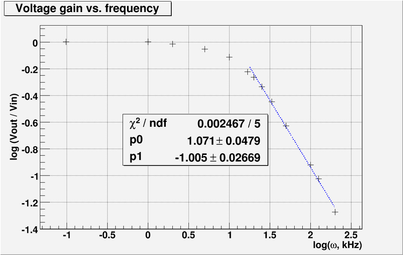
5. Graph the -vs-
phase shift (10 pnts)
- measure the phase shift between and as a function of frequency . Hint: you could use as an external trigger and measure the time until reaches a max on the scope .
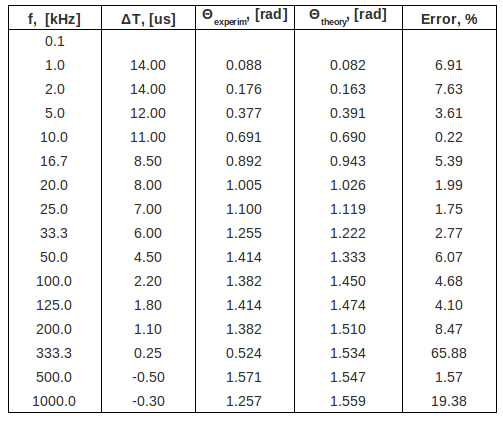
See question 4 about my phase shift measurements
Questions
1. Compare the theoretical and experimentally measured break frequencies. (5 pnts)
method 1. Using fitting line
Theoretical break frequency:
The fit line equation from the plot above is . From intersection point of line with x-axis we find:
The error is:
method 2. Using the -3 dB point
At the break point the voltage gain is down by 3 dB relative to the gain of unity at zero frequency. So the value of . Using this value I found from plot above . So . The error in this case is
2. Calculate and expression for as a function of , , and . The Gain is defined as the ratio of to .(5 pnts)
We have:
Dividing second equation into first one we get the voltage gain:
And we are need the real part:
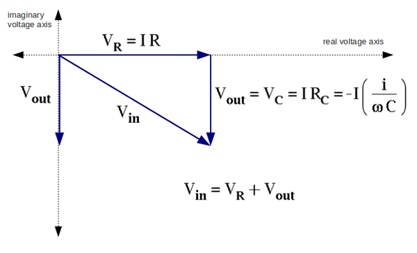
3. Sketch the phasor diagram for ,, , and . Put the current along the real voltage axis. (30 pnts)
4. Compare the theoretical and experimental value for the phase shift . (5 pnts)
The experimental phase shift is
The theoretical phase shift is
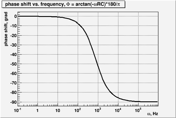
5. What is the phase shift for a DC input and a very-high frequency input?(5 pnts)
Because a DC circuit doesn't have any oscillation there are no any phase shift.
For a very high frequency input the phase shift is -90 degree (see plot in question 6)
6. Calculate and expression for the phase shift as a function of , , and graph -vs . (20 pnts)
From the phasor diagram above (question 3) the angle between vectors and given by


