Difference between revisions of "Warren Parsons Log Book"
| Line 1,657: | Line 1,657: | ||
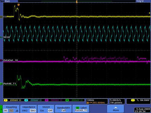
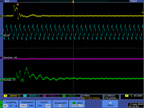
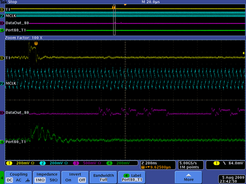
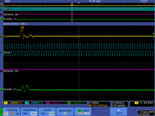
[[File:Rev3Port96.png|600px]] | [[File:Rev3Port96.png|600px]] | ||
| + | =10/3/09= | ||
[http://wiki.iac.isu.edu/index.php/User_talk:Parswarr Go back] [[User_talk:Parswarr]] | [http://wiki.iac.isu.edu/index.php/User_talk:Parswarr Go back] [[User_talk:Parswarr]] | ||
Revision as of 21:34, 3 October 2009
This tracks My Daily Progress developing the VFAT readout
VFAT2 Manuals
5/14/09
Firmware
Today we started looking at the VHDL firmware programs from Ben Raydo at JLab. Our goal: To determine what the general description of the firmware program is and determine an outline of its functionality.
Quartus II
Quartus II has a fairly good tutorial for usage. My goal is to complete this tutorial by the end of the week.
I also started to familiarize myself with the VHDL programming language.
5/15/09
Spent vast majority of day learning VHDL syntax.
Spent some time reviewing the GEM Readout Controller Firmware Status
Spent some time reviewing the v1495 instruction manual ( the Quartus II instructions in particular )
Spent some time reviewing the VFAT instruction manual
- Is there a primer somewhere on how to communicate via/with VME?
- How about this http://www.vita.com/vmefaq.html
I need to write down how to get into the DAQ as well as ROC xterm windows.
- Tamuna can show you the above
5/18/09
- From the manual on the VFAT2
- Are we using the Roman Pots or the GEM version for the channel assignments? (I assume the latter.)
GEM version
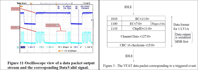
If I understand the underlying functionality of the output of the VFAT2 then the basic idea is that it transfers the hit data from SRAM1 to SRAM2 as soon as there is a LV1A signal (100) sent to the VFAT2 via the "T1" line (after the latency time programmed into the Latency Register with a default setting of 6.4us).
I thought the max latency is 6.4 us and the default is zero
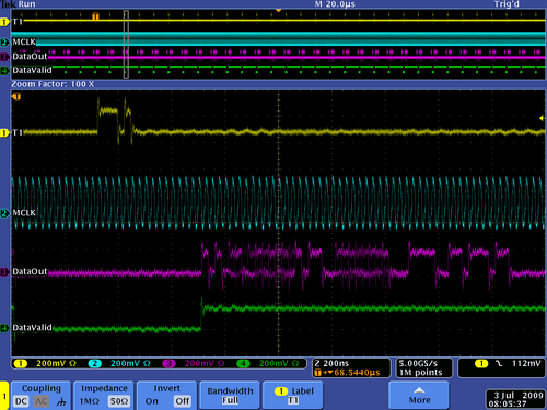
Once data is transferred from SRAM1 to SRAM2 it immediately starts outputing the information on "DataOut" at the "MCLK" rate of 40Mhz (I assume to be ultimately governed by the v1495). Valid data can be found on the "DataOut" line as long as the "DataValid" line is high. Thus the LV1A signal on "T1" followed by a transition to high on the "DataValid" line should set off the v1495 data capturing routine. Data is clocked out in FIFO order if more LV1A signals are sent to the VFAT2 before all of the data has been transferred out of the VFAT2.
I am unclear if the V1495 firmware is programmed to begin a read when the LV1A
trigger transitions or when DataValid transition.  I think it should be when
DataValid transitions.
Tamuna and I tried to log onto the ROC from scratch, but the ROC keeps saying that it can't find some boot file. I started to look through the ROC file on Dr. Forest's wiki pages, but I do not find this to be a straightforward process of rebooting the ROC. The following entry is related, and it may be helpful.
- Would it be useful to purchase the VMEbus Handbook, 4th Edition by Wade Peterson? I have personally never worked with such a complicated system with so few written resources as the VME system. I have now read quite a bit about the history of the VME system, and yet I have yet to be able to read anything on how to actually use this system. How does one begin to even crack into this system? It is a full-blown microcontroller complete with its own operating system including the complete gamut of hardware and software.
- Where did we get this Quartus II software from and why has the 30-day trial period run out? This may be making it so I cannot compile a project and get it loaded into the v1495 via the ROC. I get this impression from the fact that when I attempt to compile the project only one error comes up and that is that the 30-day evaluation period has expired. Do we have a license for it somewhere?
Licenses are free. see
http://wiki.iac.isu.edu/index.php/Qweak_V1495_FPGA_Programming
for the download page
5/19/09
Tamuna, Brian, and I worked on trying to fix the MVME6100 but to no avail. I think it's actually getting worse the more we try to get it working. We may need to wait until Dr. Forest returns before attempting to fix it. I plan on reading some more information that I found on the whole VME system as well as the MVME6100 and its associated OS, VXWorks, which is apparently used in a lot more applications than I was previously aware.
I was able to contact Ben Raydo. Thankfully he had given me quite a few suggestions on how to get started with the v1495 side of this project. I am sifting through the information he has given me.
I have found much more information on the VME system today including information on the MVME6100 (as already stated) as well as other documentation.
5/20/09
I had to brush up a bit on Verilog to figure out what was going on in the v1495usr_hal.vqm file because it is written in Verilog HDL. I have added its description above.
By whatever mystical powers the ROC is apparently now working again. I would however like to know exactly what happened to get it working.
I still need a license for Quartus II in order to continue working directly on the v1495. However, I did spend a great deal of time reading how to use the MVME6100 as well as the v1495.
5/21/09
I was able to figure out how to get the license for Quartus II and to compile an .rgb file that can be loaded into the v1495 USER FPGA. I was not aware before that we already had a completely working firmware version for the v1495 USER FPGA.
- In looking through the VHDL code to figure out how it works I have made the following discoveries
- The code in GEMReadout.vhd governs the behavior of the GEMReadout component.
- Code governing the G0 (Gin(0)) and G1 (Gin(1)) Inputs
- In GEMReadout.vhd the signal GIN(1) gets loaded into HARD_TRIGGER. HARD_TRIGGER then gets loaded into the HARD_TRIGGER of the GEMTrigger component as well as the HARD_TRIGGER of a GEMTxChannel component. Thus far I am unclear what is done with this HARD_TRIGGER signal for these components. I will figure this out on Friday, hopefully.
- Still in GEMReadout.vhd the GIN(0) signal gets loaded into the inclk0 value of the PLLBlock component. In PLLBlock.vhd (which governs the behavior of the PLLBlock component), this c0 signal eventually ends up being connected to clk(0) for the altpll component. The altpll component appears to be a predefined cell in Quartus II. I hypothesize that this component is just a pll with user-defined settings. Hopefully on Friday I can find some documentation on this component to figure out exactly how it works. Thus in GEMReadout.vhd we put in our original signal G0 and get out a locked version on PLLCLK.
- This appears to be in GEMReadout.vhd where the process trigger PLLCLK is generated. All other components that take this value in on one of its ports has it as an input rather than an output.
- nLBRES is a system-wide asyncronous reset
- LCKL is a local bus clock
- I cannot figure out where this is being generated because I lose its trail into the v1495usr_hal.vqm file going to
5/22/09
altpll is indeed an Altera Megafunction. inclk0 is the reference clock to the output clocks c0 and c1. c0 is exactly in phase with inclk0 which appears to be running at a nominal frequency of 32Mhz which as stated before ultimately ends up being the PLLCLK signal in the GEMReadout block. c1 is a phase shifted version of inclk0. Although it states that this ends up being PLLCLK_90 in GEMReadout.vhd, it is actually 180 of phase shift, i.e. an inverted clock pulse. I don't know why it was given this name since it doesn't make sense.
These calculation can be done using the input parameters to the altpll plock in the PLLBlock.vhd code from the following lines.
altpll_component : altpll GENERIC MAP (
- clk0_divide_by => 1,
- clk0_duty_cycle => 50,
- clk0_multiply_by => 1,
- clk0_phase_shift => "0",
- clk1_divide_by => 1,
- clk1_duty_cycle => 50,
- clk1_multiply_by => 1,
- ;clk1_phase_shift => "15625", <-- This is the phase shift in ps.
- compensate_clock => "CLK0",
- ;inclk0_input_frequency => 31250, <-- This is the input frequency given as the period in ps.
- intended_device_family => "Cyclone",
- invalid_lock_multiplier => 5,
- lpm_hint => "CBX_MODULE_PREFIX=PLLBlock",
- lpm_type => "altpll",
- operation_mode => "NORMAL",
The units for the frequency cannot be found in the literature. The way I figured this out was to create an altpll Megafunction block with a strange frequency. After it generated the VHDL code for the megafunction I was able to see that the output of the inclk0_input_frequency was in ps.
5/26/09
- On the question of I/O Levels.
- There are two different pin voltage levels to consider here: the I/O levels coming into the board and the I/O levels of the Cyclone chip.
- The input levels going into G0 and G1 are LVTTL (3.3V). This information, as well as the pin output assignments, are located under the menu "Assignments->Pins" in the Quartus II program.
- This information is part of the project that was created for this design. What that means is that it is not enough to just import the text files for this project and compile it. One needs the project file ".qfp" which has all of the proper pin assignments including location and levels.
- The I/O levels going into and out of the v1495 is much more difficult to ascertain. The following is an example from the GEMReadout.vhd file which programs the levels as well as whether a pin is input or output.
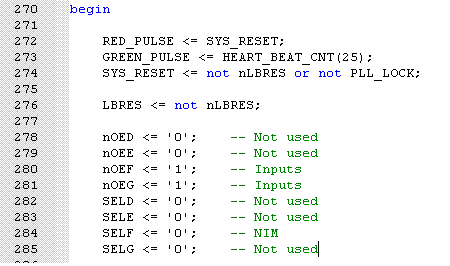
- The nOEx signals are whether or not a bidirectional pin is configured as an output or an input. A logic level "0" is an input.
- The SELG signals are whether or not a pin is TTL or NIM on the G I/Os. A logic level "0" indicates that this is a TTL level.
- The preceeding was gleaned from the v1495usr_demo project that can be downloaded for free from CAEN. There must be some hardware external to the Cyclone chip but still on the v1495 that selects these settings.
- Thus far I have not found the documentation that demostrates how this is actually done. Like I said before, at this point I have only been able to glean the information from the v1495user_demo project. Therefore, it would not surprise me if this information was somewhat faulty.
The following code was used to see if I could turn off the Red LED:
RED_PULSE <= SYS_RESET;
GREEN_PULSE <= HEART_BEAT_CNT(25);
-- SYS_RESET <= not nLBRES or not PLL_LOCK;
After resetting the VME crate, it appears to have worked. I was previously under the impression that one did not have to bump the power on the v1495 to get it to use its new firmware. I will have to explore this.
The rate at which the Green LED blinks is based off of the following code out of GEMReadout.vhd.
signal HEART_BEAT_CNT : std_logic_vector(25 downto 0);
process(LCLK, nLBRES)
 begin
  if nLBRES = '0' then
   HEART_BEAT_CNT <= (others => '0');
  elsif rising_edge(LCLK) then
   HEART_BEAT_CNT <= HEART_BEAT_CNT + 1;
  end if;
end process;
Basically what these lines of code are saying is that HEART_BEAT_CNT is a 26-bit register that originally gets set to '0'. On either a change in LCLK or nLBRES and if LCLK is a rising edge, then the HEART_BEAT_CNT gets incremented by one. From the lines of code shown before this block, GREEN_PULSE is set if the MSB of HEART_BEAT_CNT is set. Therefore, the Green LED should blink at a 50% duty cycle of 2^(25)*(20Mhz)^(-1) = 3.35 s for a 20MHz PLL frequency (i.e. on for 1.67s, off for 1.67 s).
Tomorrow I will need to determine what the signals "SYS_RESET, nLBRES, and PLL_LOCK" actually are and what they mean. As I have alluded to before, I loose the trail for many of these signals at the Cyclone package level and can only infer what their actual purposes are at this point based on the code from the GEMReadout as well as the v1495usr_demo.
5/27/09
I then doubled the PLL frequency to see if it would double the rate at which the LED was blinking. It worked.
- What this means is that the LCLK signal is somehow internal to the chip and has nothing to do with the signal that is being injected on G0.
I then changed the code back on the RED LED to see if I could restore the RED LED status with the new faster GREEN LED rate.
- This worked as well.
I attempted to change the firmware back to the original 20MHz configuration, but it does not seem to have slowed down the blinking GREEN LED at all. I am wondering if the 20MHz version was somehow corrupted. I will recompile and send this over to see if I can slow the blinking GREEN LED down.
 Note: This is because the Green LED depends on the system "LCLK" rather
than the "PLLCLK" which is supposed to be a reflected version of the G0 input.
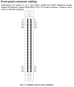
The following multipin connector settings can be found in the v1495 user manual and show explicitly where the proper pin connections can be made.
For my last item of the day I attempted to reset the Green LED to blink with "PLLCLK" rather than "LCLK." This only led to the Green LED remaining solid. This, as well as our previously failed attempts to lock with the frequency of the PLL, seems to suggest that the v1495 is not even registering the G0 input.
5/28/09
Today I attempted to get the LED to blink to the LCLK rather than the PLLCLK. It did not work.
Later I attempted to get C(1) to output the LCLK, which drives the Green LED, rather than PLLCLK_90. This also did not work.
Both of these seem to suggest that the Cyclone chip is somehow to communicating to the I/O ports on the v1495.
5/29/09
I was able to fix the firmware uploading code so that the board now resets with the new firmware loaded as well as actually exiting the program. I did this by making the following changes to the functions in v1495.c.
int
v1495reload()
{
volatile V1495 *v1495 = (V1495 *)0xfa510000;

int
v1495reload(unsigned int baseaddr)
{
volatile V1495 *v1495 = (V1495 *)baseaddr;

int
v1495firmware(unsigned int baseaddr, char *filename, int page, int user_vme)
{
 .
 .
 .
v1495reload(baseaddr); // This loads the proper base address it for refresh

return(0);   // This used to be an exit(0) command thus never allowing the program to exit properly.
             //  I suspect that exit(0) is not a VXWorks function.
}
The following line in v1495reload is actually what resets the v1495; I was tipped off to its presence by Ben.
*Conf_Flash = 1;
Before when the address for the reload function was incorrect, the USER Config Reg was never getting a '1' written to it which is what actually resets it.
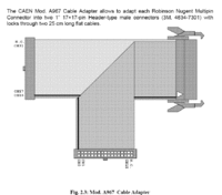
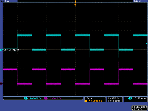
I was able to inject a 5kHz clock signal in on A(1) (since A(0) was not working on the cable from the POS-to_LVDS board) and have it output from C(3) as well as its inverse on C(5).
To do this I made the following changes to GEMReadout.vhd with which I also generated its associated .rbf file GEMReadout_A1_2_2.rbf.
-- GEM Breakout Box A CLK Signals
C(1) <= LCLK;
C(3) <= PLLCLK;
C(5) <= PLLCLK_90;
PLL_LOCK <= '1';
--PLLCLK <= GIN(0);
PLLCLK <= A(1);
PLLCLK_90 <= not A(1);
I also made the GREEN LED blink at a rate of 6.55 sec on and 6.55 sec off which was done with the following changes in code. This comes from the calculation 2^(15)*1/(5*10^3)
RED_PULSE <= SYS_RESET;
GREEN_PULSE <= HEART_BEAT_CNT(15);   -- I changed this line to the 15th bit of HEART_BEAT_CNT
SYS_RESET <= not nLBRES or not PLL_LOCK;
-- SYS_RESET <= '0';
process(PLLCLK, nLBRES) -- I changed the process sensitivity from LCLK to PLLCLK
begin
if nLBRES = '0' then
HEART_BEAT_CNT <= (others => '0');
elsif rising_edge(PLLCLK) then                -- here as well
HEART_BEAT_CNT <= HEART_BEAT_CNT + 1;
end if;
end process;
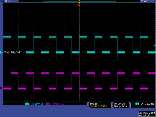
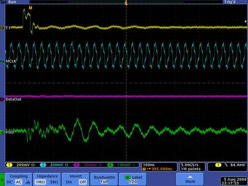
On the output of the oscilloscope below, Line2 is the output from C(3) and Line3 is the output from C(5).
When I doubled the frequency on the function generator I observed the following output on the oscilloscope as well as the GREEN LED blinking twice as fast.
This means that for some reason our input on G0 is not getting taken in. All other I/0s on the board appear to be working though!
6/1/09
I removed the bus power from the I/Os in Quartus II to see if it would kill the I/Os. It appears to not have had any effect. Apparently I did not fix anything by adding I/O bus power in the design.
- I learned today what the actual mistake was that was made on the VFAT breakout board. I have some questions relating to this mistake. There are loads of pins that are now hooked up incorrectly now. I will need to spend some time going through the manual for the VFAT to figure out what some of the settings for these pins need to be. This is most likely related to why we are having trouble getting the VFATs to communicate properly.
- What happens to the VFAT if "ScanEn" (Scan Mode Enable) is held high?
- B22 (DGND) is floating right now. Shorting it to B21 would fix it.
On a slightly different note; I need to figure out how to do a nice table in this wiki so I can enter these pin numbers in.
6/2/09
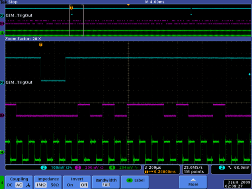
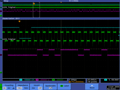
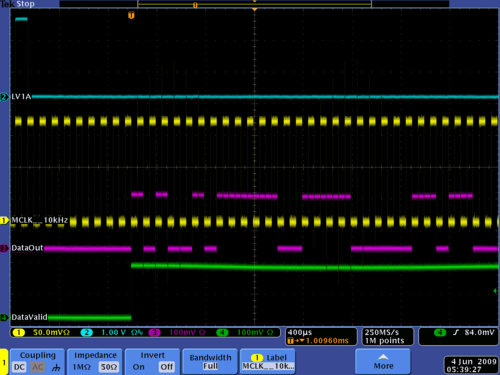
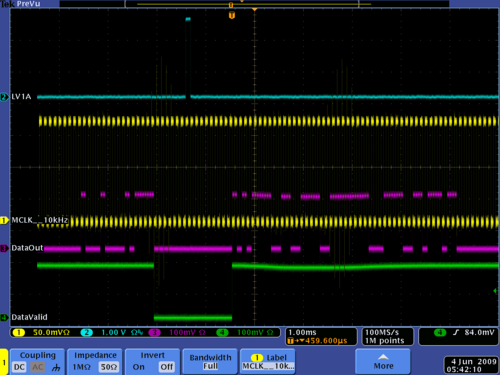
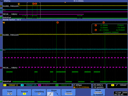
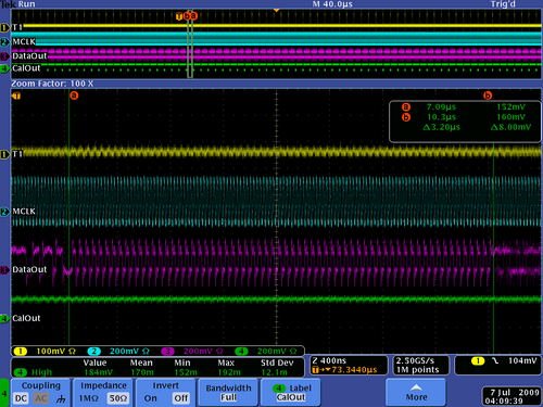
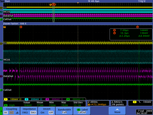
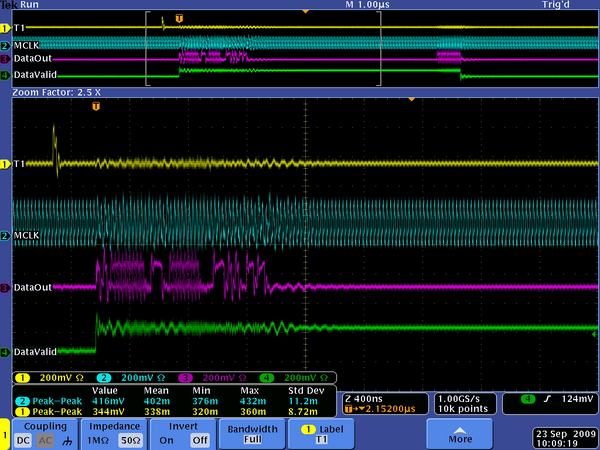
The following is the successful reading of the VFAT DF test pattern output on the DataValid, DataOut ports along with the MCLK signals ( Line 2, 3, 4 respectively). It must be noted that in order to read all of these signals at once one must disconnect the ground from the MCLK line due to its having a drastically different ground than the DataValid and DataOut signals. Since the grounds of the measured signals are effectively shorted in the oscilloscope, it attempts to balance these ground lines which it turn causes deleterious glitches in all of the signals (the MCLK glitch probably being the worst) quite often upon transistions. The first picture shows the MCLK signal with AC Coupling while the second shows the MCLK signal with DC coupling.
I was able to correct the wiring issues that I discovered yesterday; it has fixed the direct connect from the VFAT board to the breakout board. See the picture below.
The following was taken with the VFAT connected directly to the breakout board.
One disconcerting thing of note is that the bit transitions occur on the rising edge of the MCLK in these pictures, but in the documentation they are clearly supposed to transition on a falling edge. These patterns, however, appear to agree with the pictures taken previously of the DF Test Pattern. I have triple checked the polarities on these for correctness.
For some reason the notches have been taken off of the cables. The notch was originally on the positive side of the connectors. I have them connected on the negative side right now, but in the future we will most likely need to have this corrected.
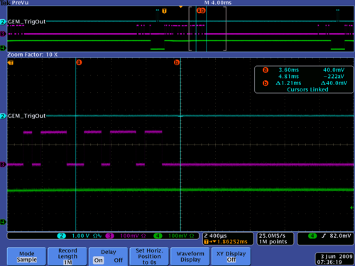
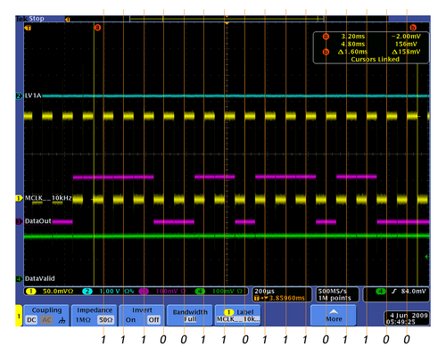
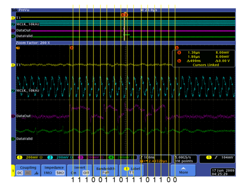
I was successfully able to pass the LV1A signal through the v1495 and request a formatted data package from the VFAT. The following shows the ChipID isolated between the two cursors. ChipID<1>=150=bin(10010110) ChipID<0>=236=bin(1101100) As per the VFAT manual, only the last four bits from ChipID<1> make it into the formatted data stream along with the full ChipID<0>.
6/3/09
All of the VFAT ports on the breakout board have been rewired and appear to be working except port 80. I still have not been able to observe a good DataOut stream from this one. I have tested several different VFATs in this port and tested the same chips in different ports, so I know that it is just the port itself. I recommend that since we will hopefully be getting a new board soon anyway that we not worry about trying to diagnose why this port is malfunctioning. Also, I noticed that with all of the peripherals disconnected there is only 10kOhm of resistance between VCC and GND. I'm wondering if in all of the resoldering that we haven't accidentally gotten some stringers across some lines somewhere or something to that effect.
The DATout pulses below represent the checksum (just before datavalid goes low) and, after datavalid goes high, the beginning of the EC, BC, flag, and CHIP ID bits.
The VFAT chip ID appears between the vertical yellow lines marked "a" and "b"below. The bits are 1110011011101100. The first 4 bits (1110) are a header and the remaining bits (011011101100 b = 6ec h) represent the CHIP ID as described in Figure 8 of the VFAT 2 manual.
6/4/09
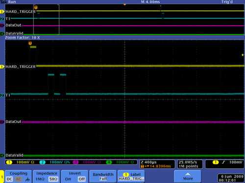
I was able to use the DG535 to send a single pulse to the Agilent 81110A to send out a single Hard Trigger pulse followed by a large number of MCLK pulses (~200).
Port 80 is now working. The MCLK- pin was not properly soldered to the connector. I found it by doing a continuity test on the pins.
The first memory address right after the v1495 base addresses are where all of the data are being stored. I did not realize this before. It is simply a matter of reading these memory locations to get the data after it has gone in. I still don't understand the exact mechanism that stores these values into these registers. It has to do with some primative memory blocks in the Cyclone chip.
This is where the value for the Hard Trigger Word is as well. Three of the bits in this word are the actual bits that get shipped out on LV1A when a Hard Trigger pulse is sent to the v1495. Right now I am just simulating this, but knowing where this value is stored, I should be able to actually get it to fire correctly.
I now understand how the read and writing mechanisms to the local bus work, however, I would probably not be able to set this up from scratch as CAEN holds the secrets as to how the actual pins from the Cyclone chip make their connections to other parts of the board. Fortunately, it is not necessary to now this level of detail for this project, and it is obvious that CAEN did this intentionally.
We were able to query several GEM-specific registers to confirm that we had been able to locate them. We were able to change the Revision number and observe the change from the ROC.
There are only a certain number of registers that are located in the GEMReadout file that are capable of being read and/or written to. If the register is not on the list and if it is written to, nothing will happen, and if it is read, all that will be output is zeros. I am not yet certain if one can add other registers if one wants to be able to query their respective contents such as the HARD_TRIGGER_WORD register which as of right now, one cannot query its contents.
6/5/09
I was successfully able to program the 3-bit HARD_TRIGGER_WORD, i.e. the word that is sent out on T1. It is located at memory location 0xaddr0014(5:3). Below I have shown how to explicitly program these three bits. Here I have programmed it to have a 1-0-1 pattern as shown in the picture below as well.
-> m 0x80110014,2
80110014:  0000-0028
80110016:  0000-.
value = 1 = 0x1
I have been able to observe the first three words being entered into the v1495 USER memory.
I created the following function in GEMReadoutCtrl.c:
void GEMSprint(void) // this function prints out my favorite registers
{
	UINT32 Addr = 0x80110000;
	volatile GEMReadoutCtrlRegs *v1495 = (GEMReadoutCtrlRegs *) Addr;

	printf("A0_EVENTDATA Addr: 0x%08x Data: 0x%04x \n",&(v1495->EventData_0[0]),v1495->EventData_0[0]);
	printf("A0_FIFOSIZE Addr: 0x%08x Data: 0x%04x \n",&(v1495->FIFOLength[0]),v1495->FIFOLength[0]);
	printf("A0_EVENTSIZE Addr: 0x%08x Data: 0x%04x \n",&(v1495->EventSize[0]),v1495->EventSize[0]);
	//printf("A0_EVENTDATA Addr:%04h Data:%04h \n",&(),);
	printf("\n");

	return;
}
This returned the following results when I ran the function three times consecutively:
-> GEMSprint()
A0_EVENTDATA Addr: 0x80114000 Data: 0xa4f0
A0_FIFOSIZE Addr: 0x80110030 Data: 0x02c0
A0_EVENTSIZE Addr: 0x80110048 Data: 0x0000

value = 1 = 0x1
-> GEMSprint()
A0_EVENTDATA Addr: 0x80114000 Data: 0xc042
A0_FIFOSIZE Addr: 0x80110030 Data: 0x0280
A0_EVENTSIZE Addr: 0x80110048 Data: 0x0000

value = 1 = 0x1
-> GEMSprint()
A0_EVENTDATA Addr: 0x80114000 Data: 0xe66c
A0_FIFOSIZE Addr: 0x80110030 Data: 0x0240
A0_EVENTSIZE Addr: 0x80110048 Data: 0x0000
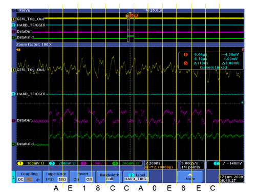
The first nibble of each word is it's respective header which are correct per Figure 8 in the VFAT manual. The last word recorded has the ChipID number 66c which is correct for this device.
See below for the oscilloscope results of the values as they are passed through the v1495. The value highlighted between the cursors is the last word recorded.
Although I was able to see this data, I am still not 100% clear on exactly how this memory is stored. It is still somewhat buggy as it will not always correctly reliquish its captured data nor the correct number of words that are in the data FIFO.
6/8/09
Having learned that the SizeFIFO length is the last six bytes of the EVENTSIZE data request (as opposed to the last eight as I previously thought), I can see that every time I request a dump of the data memory the ROC is missing two words per request. See output from ROC below:
-> GEMReset()
value = 0 = 0x0
The preceding function resets the v1495 including zeroing out both the data and the size FIFOs.
Trigger the VFAT with one pulse and now display the contents of the ROC memory
-> d 0x80110030
80110030:  0301                                      *................*
value = 21 = 0x15
The preceding function dumps the memory found at 0x80110030. This is the EventSize register which contains the number of words in the dataFIFO(15:6) and the sizeFIFO(5:0).
0x0301 = 001100000001 b
The module address 80110030 is 0x30 away from the base address 0x11.
000001 b = 1 d there is 1 event waiting in the sizeFIFO.
The remaining 10 bits 0000001100 b = 12 d = number of 16 bit words in the dataFIFO.
80110030:  0301                                      *................*
value = 21 = 0x15
-> d 0x80114000
80114000:  aa40                                      *.l..............*
value = 21 = 0x15
-> d 0x80110030
80110030:  0241                                      *.A..............*
value = 21 = 0x15
0x2401 = 001001000001 b
After reading only "one" word off of the top of the dataFIFO, the number of words reported to be in the dataFIFO has decreased to 0000001001 b = 9 d.
Is it possible that 3, 16 bit words were taken out of the FIFO?
-> d 0x80114000
80114000:  0000                                      *................*
value = 21 = 0x15
-> d 0x80110030
80110030:  0181                                      *................*
value = 21 = 0x15
Again the number of words in the dataFIFO decreases by 3 since we now have 0000000110 b = 6 d.
If I manually read out the data one at a time using a call to the contents of this register via a C function, I do not have this problem. That is why I was able to access the data last week. However, if I loop in a function to get these contents I am only able to get the first value and the dataFIFO only decrements by one. I am trying a different firmware version which only requires that the "Read Request Bit" be high (rather than a rising edge) to access the data. I'm hoping that this will fix the problem.
- This did not fix the problem; in fact it made it so the memory dump would skip by six words each time! A looping call to the value remains unchanged. I am wondering if because the value of my variable was not declared as a "volatile" that it is not letting the program actually update the value.
I am wondering if the VxWorks function "d" doesn't do some kind of repeat call of the register for bit integrity. That may be what the extra information marked by the *...* is for.
External Connections
| From v1495/ To VFAT | MCLK C(0)=>C(5)
Trig C(10)=>C(15) |
|---|---|
| From VFAT/ To v1495 | DataOut16 A(14) DataValid16 A(13)
DataOut32 A(12) DataValid32 A(11) DataOut48 A(10) DataValid48 A(9) DataOut64 A(8) DataValid64 A(7) DataOut80 A(6) DataValid80 A(5) DataOut96 A(4) DataValid96 A(3) |
| From Signal Generator/ To v1495 | MCLK A(17)->A(22)
Trig A(25)->A(31) |
v1495 Registers
In the registers below "addr" refers to the four-hex base address of the v1495. For our experiments thus far this has had the value 0x8011.
| Member of struct pGEMReadoutCtrl | Address | Bit Format | Description |
|---|---|---|---|
| FIFOLength[0] | 0xaddr0030 | FIFOdataSize<15:6> FIFOLength<5:0> | FIFOSize = number of 16 bit words in Fifio: FIFOLength = number of events of size FIFOdataSize in FIFO: example: 0x0301 = 001100000001 b => FIFOdataSize = 0000001100 d = 12, 16 bit data words, FIFOLength= 000001 b = 1 event of 12, 16 bit words in FIFO. |
| EventSize[0] | 0xaddr0048 | x"000" & EventSize<3:0> | Reading of this register gives the results off of the top of the sizeFIFO. This contains how many words were entered into the dataFIFO from the previous event. |
| EventsSentH[0]/EventsSentL[0] | 0xaddr0080/0xaddr00A0 | Each occupies whole word | This records the number of events that have occurred since the v1495 was last reset. |
| EventData[0][0] | 0xaddr4000 | Whole word | Reading of this register gives the oldest word in the dataFIFO. |
6/9/09
I was successfully able to simultaneously read the formatted data off of all six VFATs (after repairing the DataValid line on PORT 64). For reasons only known to those who programmed the ccppc, if one assigns a register to a variable outside of a for-loop and then assign that contents of that variable to another variable inside of the for-loop, the ROC will not update this original value. One has to explicitly have the final variable read out the contents of the v1495 register, or it will not automatically update them! I even tried to declare all of these variables as "volatile" in an attempt to get them to update but to no avail.
Also, this compiler has a hard time with simple pointers sometimes as well. It's something to watch out for.
In the following printout from the ROC one is able to see that after I reset the v1495 ("v1495Reset()"), I sent two events to the VFATs. These events are read in via "v1495ReadEvent()" and read out via "v1495StatusPrint()".
Right now the data is stored in a static struct on the ROC. It is a relatively simple matter to alter these functions to take in a pointer to an array of UINT32 type variables and hand off the starting address of this struct to this pointer. I can also return the size of the array from the function to communicate the size; either that or I could take a variable in that gives the size. Either way works about the same.
-> v1495Reset()
value = 0 = 0x0
-> v1495Sprint()
A0_FIFOSIZE Addr: 0x80110030 Data: 0x0602
A0_EVENTSSENT Addr: 0x801100a0 Data: 0x0001
Number of words in dataFIFO : 0024, 0x0018
Number of words in sizeFIFO : 0002

value = 1 = 0x1
-> v1495ReadEvent()
value = 1 = 0x1
-> v1495StatusPrint()
GEM[0]: #B[24] #F[1/2] B/s[24] F/s[1]
  LastCap[12]: A415 C050 E66C 0000 0000 0000 0000 0000 0000 0000 0000 56DC
GEM[1]: #B[24] #F[1/2] B/s[24] F/s[1]
  LastCap[12]: A1A5 C020 EA6C 0000 0000 0000 0000 0000 0000 0000 0000 E86D
GEM[2]: #B[24] #F[1/2] B/s[24] F/s[1]
  LastCap[12]: A1A5 C020 E8EC 0000 0000 0000 0000 0000 0000 0000 0000 447C
GEM[3]: #B[24] #F[1/2] B/s[24] F/s[1]
  LastCap[12]: A275 C030 E6EC 0000 0000 0000 0000 0000 0000 0000 0000 B338
GEM[4]: #B[24] #F[1/2] B/s[24] F/s[1]
  LastCap[12]: A1A5 C020 E8EC 0000 0000 0000 0000 0000 0000 0000 0000 447C
GEM[5]: #B[24] #F[1/2] B/s[24] F/s[1]
  LastCap[12]: A1A5 C020 E6EC 0000 0000 0000 0000 0000 0000 0000 0000 A426
value = 1 = 0x1
-> v1495ReadEvent()
value = 1 = 0x1
-> v1495StatusPrint()
GEM[0]: #B[24] #F[1/2] B/s[24] F/s[1]
  LastCap[12]: A4E5 C060 E66C 0000 0000 0000 0000 0000 0000 0000 0000 A9F8
GEM[1]: #B[24] #F[1/2] B/s[24] F/s[1]
  LastCap[12]: A275 C030 EA6C 0000 0000 0000 0000 0000 0000 0000 0000 FF73
GEM[2]: #B[24] #F[1/2] B/s[24] F/s[1]
  LastCap[12]: A275 C030 E8EC 0000 0000 0000 0000 0000 0000 0000 0000 5362
GEM[3]: #B[24] #F[1/2] B/s[24] F/s[1]
  LastCap[12]: A345 C040 E6EC 0000 0000 0000 0000 0000 0000 0000 0000 0BCB
GEM[4]: #B[24] #F[1/2] B/s[24] F/s[1]
  LastCap[12]: A275 C030 E8EC 0000 0000 0000 0000 0000 0000 0000 0000 5362
GEM[5]: #B[24] #F[1/2] B/s[24] F/s[1]
  LastCap[12]: A275 C030 E6EC 0000 0000 0000 0000 0000 0000 0000 0000 B338
value = 1 = 0x1
-> v1495ReadEvent()
value = 0 = 0x0
-> v1495StatusPrint()
GEM[0]: #B[0] #F[0/2] B/s[0] F/s[0]
  LastCap[0]:
GEM[1]: #B[0] #F[0/2] B/s[0] F/s[0]
  LastCap[0]:
GEM[2]: #B[0] #F[0/2] B/s[0] F/s[0]
  LastCap[0]:
GEM[3]: #B[0] #F[0/2] B/s[0] F/s[0]
  LastCap[0]:
GEM[4]: #B[0] #F[0/2] B/s[0] F/s[0]
  LastCap[0]:
GEM[5]: #B[0] #F[0/2] B/s[0] F/s[0]
  LastCap[0]:
value = 1 = 0x1
From the middle two nibbles in the second word of each output, one can see the Event Counter incrementing by one. Also, from the last three nibbles from the third word of each output one can see the ChipID from each VFAT. I had not noticed it before but these three nibbles are not unique. From the output one can see that one pair shares the ChipID 8EC and another pair shares the ChipID 6EC. This was confirmed by looking up the ChipIDs from each these VFAT's respective website.
6/10/09
I spent the vast majority of the day just figuring out how the v792 files were created so we can create our own v1495 with an extremely similar format.
6/11/09
VxWorks API Reference : OS Libraries
Useful description of the vxMemProbe function for VxWorks:
vxMemProbe( )

NAME

    vxMemProbe( ) - probe an address for a bus error

SYNOPSIS

    STATUS vxMemProbe
        (
        char * adrs,              /* address to be probed */
        int    mode,              /* VX_READ or VX_WRITE */
        int    length,            /* 1, 2, 4, or 8 */
        char * pVal               /* where to return value, or ptr to value */
                                  /* to be written */
        )

DESCRIPTION

    This routine probes a specified address to see if it is readable or writable, as specified by mode. The address is read or written as 1, 2, or 4 bytes, as specified by length (values other than 1, 2, or 4 yield unpredictable results). If the probe is a VX_READ (0), the value read is copied to the location pointed to by pVal. If the probe is a VX_WRITE (1), the value written is taken from the location pointed to by pVal. In either case, pVal should point to a value of 1, 2, or 4 bytes, as specified by length.

    Note that only bus errors are trapped during the probe, and that the access must otherwise be valid (i.e., it must not generate an address error).

EXAMPLE

        testMem (adrs)
            char *adrs;
            {
            char testW = 1;
            char testR;

            if (vxMemProbe (adrs, VX_WRITE, 1, &testW) == OK)
                printf ("value %d written to adrs %x\n", testW, adrs);

            if (vxMemProbe (adrs, VX_READ, 1, &testR) == OK)
                printf ("value %d read from adrs %x\n", testR, adrs);
            }

MODIFICATION

    The BSP can modify the behaviour of vxMemProbe( ) by supplying an alternate routine and placing the address in the global variable _func_vxMemProbeHook. The BSP routine will be called instead of the architecture specific routine vxMemArchProbe( ).

RETURNS

    OK, or ERROR if the probe caused a bus error or was misaligned.
I need to study this function as it is one of the only ones left that I don't understand from the c792 code. I should be able to figure out how to use it pretty quickly tomorrow.
I figured out how the addressing works for the v1495: the three dials are the base address settings for the A32<31:16> VMEbus address. I was able to use the function sysBusToLocalAddr() to assertain that the Local address 0x80110000 is 0x78000000 higher than the VMEbus address 0x08110000. Something wasn't quite making sense about this before.
I have also located some truly unique identifiers for our v1495. There is an IEEE OUI (a hex number assigned to CAEN by IEEE), a BoardID number unique to the v1495 card, as well as a serial number (this one I am assuming is the most unique i.e. for our particular board). We should be able to use these values in the init function to make sure we are properly communicating with the v1495. The only difficultly with where these are located is that they are not in the FGPA USER registers. They are in the Configuration ROM which is separated from the base address by quite a ways. I believe it is going to be easier to set up a defined offset to locate these values rather than use reserved values in the struct definition.
6/12/09
I have noticed that if the input to the DataOut and DataValid are left open the signal is interpreted as a high signal. Furthermore, when the VFATs are first plugged in these ports are still left open (or forced high although I can't be sure). We can use this fact to our advantage by sending a dummy LV1A request to the VFATs and then reset the v1495 to see if their EVENTS_SENT > 0. It is a handy "glitch" in the v1495 firmware that if the DATA_VALID line is high after a reset, it increments the EVENTS_SENT value. Therefore, if they are working then the EVENTS_SENT should equal zero.
The reason that the v1495Init(...) function wasn't working immediately after reboot was that the values for the DataValid and DataOut were not being taken into the v1495 until the original MCLK was being run. Furthermore, they start off initialized to zero in the firmware. Making the process that controls reading DataValid and DataOut depend on Reset as well will fix this.
- I cannot remember the syntax for transferring files using the pscp program on the Windows computer. I tried the following but to no avail:
- pscp GEMReadout_All.rbf daq@daq1:134.50.3.210
You need to add a ":" at the end it should look like this
- pscp GEMReadout_All.rbf daq@daq1:134.50.3.210:
I got it to work using the following syntax:
pscp GEMReadout_All.rbf daq@134.50.3.210:
- How does one figure out the IP address of the computer in the tcsh shell, by the way?
/sbin/ifconfig
Ah excellent. This worked nicely.
Also, I was wondering if we shouldn't make reseting the VFATs possible using the v1495. This may be something that we should include into the next breakout board rev if it isn't already there.
6/15/09
Last week I did not anticipate that it would crash the ROC while attempting to debug my array transfer function. Today I am going to practice using another generic 32-bit array to practice with. Hopefully, this won't be as prone to crashing.
This worked as Dr. Forest and I were able to get the data successfully transferred into a CODA data file.
I now have the GIN ports working. There was this nasty Cyclone LE (Logic Element) called cyclone_lcell that the TTL/NIM control bit was going into. Of course there is almost no documentation available on these lcells. I - as did those who wrote the original GEM firmware - assumed that all this did was buffer the signal. I noticed that hidden in this LE was a phrase that hinted that rather than buffer the signal, it inverted it. So after all of that digging, all I ended up having to do was invert the signal going to the TTL/NIM control bit.
Please document how this works in your thesis.
Let's set up a logic unit to take the and of a trigger
pulse  and the clock.  The output pulse will go into G1
and trigger the VFATsr G1

Lets use a TTL input for G0 and G1

ca
6/16/09
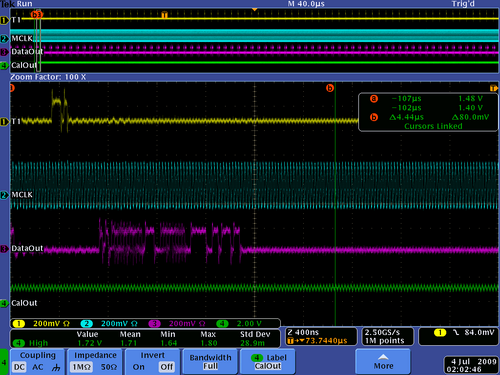
The following is the output from GEM[0] with an MCLK of 32Mhz. As hoped, the RED LED on the V1495 goes out when the PLL locks with the incoming MCLK from the pattern generator.
I have zoomed in on the ChipID to show that they match (ChipID from GEM[0] is 0x6EC). All of the signals shown are actually buffered signals of the originals as they are passed through the V1495. The HARD_TRIGGER signal does not have to be in sync with the MCLK. As long as it is at least 1.5 periods of the MCLK, I think we will be okay. Also, the CAEN N405 can apparently only produce a maximum pulse width of 200ns (it says 800ns in the manual). Putting all of this together means that we can probably go no slower than 6.5Mhz with this setup.
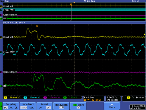
It was somewhat difficult to time this circuit correctly, but I was able to capture an event that was triggered off of the GEM_Trig_Out: the output of the GEM amplifier.
The following was the printout from the v1495StatusPrint() function corresponding to this cosmic event. It appears that we will most likely have to calibrate the lines as well as set up the pulse-shaping in order to get any valid reads on any of the lines; they are all zero here.
   -> v1495StatusPrint()
V1495[0]: #B[24] #F[1/22] B/s[24] F/s[1]
  LastCap[12]: AE18 CCA0 E6EC 0000 0000 0000 0000 0000 0000 0000 0000 9B6A
Event Count: 202 ; Chip ID : 0x6EC
V1495[1]: #B[24] #F[1/25] B/s[24] F/s[1]
  LastCap[12]: ACAE C9A2 EA6C 0000 0000 0000 0000 0000 0000 0000 0000 72DF
Event Count: 154 ; Chip ID : 0xA6C
V1495[2]: #B[24] #F[1/28] B/s[24] F/s[1]
  LastCap[12]: AA9A C2D2 E66C 0000 0000 0000 0000 0000 0000 0000 0000 3CFC
Event Count: 45 ; Chip ID : 0x66C
V1495[3]: #B[24] #F[1/30] B/s[24] F/s[1]
  LastCap[12]: AC14 C9A2 E8EC 0000 0000 0000 0000 0000 0000 0000 0000 BAF1
Event Count: 154 ; Chip ID : 0x8EC
V1495[4]: #B[24] #F[1/33] B/s[24] F/s[1]
  LastCap[12]: ACB5 C993 E6EC 0000 0000 0000 0000 0000 0000 0000 0000 1B25
Event Count: 153 ; Chip ID : 0x6EC
V1495[5]: #B[24] #F[1/36] B/s[24] F/s[1]
  LastCap[12]: A9A3 C1A2 E8EC 0000 0000 0000 0000 0000 0000 0000 0000 F0A8
Event Count: 26 ; Chip ID : 0x8EC
I have zoomed in on the first three words of the data package from GEM[0] to show that they match. Also, ground and cross-talk is showing up particularly when data is being read out of the VFATs. Even with a few minor adjustments we were able to get it mostly under control. With a little more careful planning, I think we should be able to run the MCLK at 32 Mhz without any major issues.
At some point I will need to return the 32 MHz pulse generator.
My Stanford pulse generator only goes up to 999 kHz pulse .
We need a configuration which will do 500 kHz.
I think we can find a way to increase the LV1A trigger pulse width.
Let's have 2 firmware versions, one at 32 MHz requiring PLL and one at 500 kHz.
- The limitation on the frequency is a function of the maximum pulse width that the CAEN N405 can do since we need the output pulse for the HARD_TRIGGER to be high for at least one period of the MCLK. If we can trigger the Stanford pulse generator with the NIMs equipment then we are in business to do a much lower frequency. I can't remember off hand what the lower end of the PLL was. Either way works just fine with the timing since I'm sure the designers did their homework to figure out what the lowest frequency was that didn't need a PLL to maintain a clean signal.
I will need to use the Stanford pulse generator as
as MCLK.  We can send the N405 output pulse into a
gate generator and increase the pulse width.
6/17/09
I have been attempting to figure out the algorithm behind the CRC-16 word at the end of the transmission. It is promised on the web and other places that the computation for these are fairly efficient, and we may be able to use this to make sure that our data transmissions are intact.
I was able to add code to the v1495ReadEvent() function that prints off the hits on the individual channels. We can possibly reuse some of this code when we go to implement our GUI with the hits on it. It basically takes a hex number and parses it out into four hex numbers making it appear like a binary number. It actually ends up taking four times more memory to store this information so it is for reading out convenience only. The following shows the output of the new function implemented on the ROC.
I have attempted to make this code very efficient, so reading it to figure out what's going on might be somewhat painful.
-> v1495ReadEvent()
v1495ReadEvent: Data entered into v1495Channel[0]
Channels 1 -> 32: 0000 0000 0000 0000 0000 0000 0000 0000
Channels 33 -> 64: 0000 0000 0000 0000 0000 0000 0000 0000
Channels 65 -> 96: 0000 0000 0000 0000 0000 0000 0000 0000
Channels 97 -> 128: 0000 0000 0000 0000 0000 0000 0000 0000
v1495ReadEvent: Data entered into v1495Channel[1]
Channels 1 -> 32: 0000 0000 0000 0000 0000 0000 0000 0000
Channels 33 -> 64: 0000 0000 0000 0000 0000 0000 0000 0000
Channels 65 -> 96: 0000 0000 0000 0000 0000 0000 0000 0000
Channels 97 -> 128: 0000 0000 0000 0000 0000 0000 0000 0000
v1495ReadEvent: Data entered into v1495Channel[2]
Channels 1 -> 32: 0111 0111 1111 0111 0111 0111 0101 0101
Channels 33 -> 64: 1101 1101 1111 1111 0111 1111 1101 0101
Channels 65 -> 96: 1101 0101 0101 1101 0101 1101 1111 0101
Channels 97 -> 128: 0101 0111 1111 0101 0101 1011 0001 0100
v1495ReadEvent: Data entered into v1495Channel[3]
Channels 1 -> 32: 0000 0000 0000 0000 0000 0000 0000 0000
Channels 33 -> 64: 0000 0000 0000 0000 0000 0000 0000 0000
Channels 65 -> 96: 0000 0000 0000 0000 0000 0000 0000 0000
Channels 97 -> 128: 0000 0000 0000 0000 0000 0000 0000 0000
v1495ReadEvent: Data entered into v1495Channel[4]
Channels 1 -> 32: 0000 0000 0000 0000 0000 0000 0000 0000
Channels 33 -> 64: 0000 0000 0000 0000 0000 0000 0000 0000
Channels 65 -> 96: 0000 0000 0000 0000 0000 0000 0000 0000
Channels 97 -> 128: 0000 0000 0000 0000 0000 0000 0000 0000
v1495ReadEvent: Data entered into v1495Channel[5]
Channels 1 -> 32: 0000 0000 0000 0000 0000 0000 0000 0000
Channels 33 -> 64: 0000 0000 0000 0000 0000 0000 0000 0000
Channels 65 -> 96: 0000 0000 0000 0000 0000 0000 0000 0000
Channels 97 -> 128: 0000 0000 0000 0000 0000 0000 0000 1000
value = 84 = 0x54 = 'T'
-> v1495StatusPrint()
V1495[0]: #B[24] #F[1/2234] B/s[24] F/s[1]
  LastCap[12]: A025 C870 E6EC 0000 0000 0000 0000 0000 0000 0000 0000 C99B
Event Count: 135 ; Chip ID : 0x6EC
V1495[1]: #B[24] #F[1/2234] B/s[24] F/s[1]
  LastCap[12]: A9B9 CD32 EA6C 0000 0000 0000 0000 0000 0000 0000 0000 16CE
Event Count: 211 ; Chip ID : 0xA6C
V1495[2]: #B[24] #F[1/2234] B/s[24] F/s[1]
  LastCap[12]: A6C7 C552 E66C 77F7 7755 DDFF 7FD5 D55D 5DF5 57F5 5B14 6D77
Event Count: 85 ; Chip ID : 0x66C
V1495[3]: #B[24] #F[1/2234] B/s[24] F/s[1]
  LastCap[12]: A807 C652 E8EC 0000 0000 0000 0000 0000 0000 0000 0000 0EA1
Event Count: 101 ; Chip ID : 0x8EC
V1495[4]: #B[24] #F[1/2234] B/s[24] F/s[1]
  LastCap[12]: A39A C193 E6EC 0000 0000 0000 0000 0000 0000 0000 0000 30A4
Event Count: 25 ; Chip ID : 0x6EC
V1495[5]: #B[24] #F[1/2234] B/s[24] F/s[1]
  LastCap[12]: A2FE C020 E8EC 0000 0000 0000 0000 0000 0000 0000 0008 8AE2
Event Count: 2 ; Chip ID : 0x8EC
value = 33 = 0x21 = '!'
Let's start taking cosmic data overnight

I tried to turn everything back on but the
V1495 didn't seem to lock with the pulse generator.
The left led was blinking red/green

I set the VFAT cards up to have different thresholds.
We will want to start studying VFAT preamp values and threshold
to determine the optimal setting
6/18/09
I have learned how to write programs that work on the Gumstix computer. I have redone the stop.arm and run.arm to turn off and turn on all of the VFATs respectively. I have nearly finished remodeling the flipbit.arm program so that one can flip either a single bit or an entire register at once. I just need to tidy up it's functionality with the extended registers. If one were to use it right now on the extended registers, I'm not sure what it would do actually. I think that it would just try to write on the base register. In any case, I should have this working early tomorrow morning.
Also, I talked to Brian and was wondering if getting the new breakout boards or the better/more interactive website for the VFATs working would be better. My vote is for the website for the VFATs, but I'm not 100% sure on the time lines and other pertinent factors.
I think we want to put priority on getting the new breakout boards in
We may still find errors which need to be fixed.
Although it is inconvenient we can probably limp
along with the VFAT controls we have now
programming controls as needed.
6/19/09
I spend the morning debugging why the I2C wasn't working. After having communicated with Brian on the issue, I determined that one of the VFATs - for whatever reason - was holding down the SDA line. This rendered attempted communication by the VFATs moot.
I have rewritten the flipbit.arm program so that one can change an entire register at a time rather than just one bit at a time. The format of the entry has slightly changed but is included in the help documentation for the program itself which is also shown below.
Input file should be of the form:
<mode> <base address> <register address> <bit or hex value> <action>
<mode>: either "p" for primary or "e" for extended
<base address>: this is the base I2C address for the VFAT
<register address>: this is the respective I2C address for the VFAT
<bit or hex value>:
         if bit then {1..7}
         if hex then {0x00..0xFF}
<mode>: "on" turn the bit(s) on.
         "off" turn the bit(s) off.
         "flip" flip the bit(s).
        "set" set the bits as the hex value.
As an example:
echo "p 32 0 0x01 on" | ./flipbit.arm

or

echo "p 32 0 0 on" | ./flipbit.arm
Either or these would cause the sleepb mask for VFAT at I2C address 32 to turn on (thus turning on the VFAT).
echo "e 96 134 0x10 on" | ./flipbit.arm

or

echo "e 96 134 4 on" | ./flipbit.arm
Either of these would turn on the DFTestPattern for the VFAT at I2C address 96.
Where it becomes really nice is in the following example:
echo "p 80 2 0xFF on" | ./flipbit.arm
This would cause the IPreAmpin register to have a value of 0xFF (0d255) in one fell swoop.
There is no equivalent for doing this with one command with the old flipbit.arm program.
echo "p 80 4 0xAA set" | ./flipbit.arm
This would set the value in the IPreampOut register to 0xAA (0b1010_1010) regardless of what the previous value was.
- Important!*
Adding the "-n" suffix to the end of ./flipbit.arm now kills the verbose output. The VFAT.setup script is setup with this, so if one runs it right now, you won't see anything getting printed to the Gumstix xterm window.
Before leaving I turned off all of the VFATs. If you run the script it will turn them back on.
I wasn't sure if everything else was set up and ready to start taking data. If it is I can go back and start up CODA. If all I need to do is hit the "run" button, I'm sure I can manage. If I have to start up any of the other terminals I probably won't know what I'm doing.
I tried to start the DAQ but the ROC appears to be crashing.
Perhaps I am downloading the wrong ROC lib.
Lets clean up the ROC lib directory and try on Monday
Once everything is going lets leave it on.
6/22/09
Location of the test.dat file reader.
/home/daq/CODA/CODAreader/UsingROOTnEVIO/VFAT
6/23/09
The following is the current I2C address with its respective ChipID
| I2C | ChipID |
|---|---|
| 16 | 0x6EC |
| 32 | 0xA6C |
| 48 | 0x66C |
| 64 | 0x8EC |
| 80 | 0x6EC |
| 96 | 0x8EC |
6/24/09
The VFAT threshold tests show an ability to set the threshold high enough that no hits will be recorded. There is definitely a correlation to be seen between the value of Threshold_1 and the number of all zero events and the average number of hits per event. Right now there is a trade off between the targeted .75 all zero hits percentage for VFATS 0, 1, 4, and 5 as well as the .50 all zero hits percentage for VFATS 3 and 4 and the average number of hits recorded for each event where the VFAT has at least one hit recorded.
There are still several areas of concern for me on this project, and that I believe we will be forced to tackle if we are going to get what we want from it.
First, I would personally like to have a much, much better understanding of the processes involved in the triggering signal.
The trigger is currently being generated by the last GEM foil stage.  The charge leaving
the last GEM foil for the charge collector is sourced by the last GEM foil.  This charge loss
appear as a current drop on the last GEM foil.  This current drop produces a pulse which is inverted
by an OP amp and sent to a Constant Fraction Discriminator.
Before I start rambling about specifics let me ask if there is any documentation on this detector or these detectors in general. I suppose I could lump making sure that we intimately understand all of the setting we have for the trigger. For instance, if it is correct that the dE/dx for the particles we are measuring are so similar, then why are we seeing spikes from the trigger line that can be as much as twice the size of each other (i.e. the pulse from the detector can vary as much as 232mV from the detector)? Isn't the varying amplitude of these spikes a function of the varying energy lost by the particles in the detector? What other factor(s) would account for this? If there are other factors I'm not aware of, would it be possible to filter them out?
Second, we need to also intimately understand the settings for the filter and amplifiers on these channels. I have uncovered some documentation on these, but it may not be enough to understand what is going on. Are there contacts at CERN whom we can contact about this device? Is it possible that there are people at JLAB who also know about these parameters? I see lots of names attached to these papers; I wonder if they are reachable.
Finally, what are the future plans for setting up calibration for the VFATs? I see that there is the possibility to externally measure the voltage and current setting for the amplifiers/filters. How important do we reckon these parameters will be in the final design?
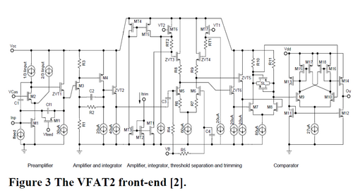
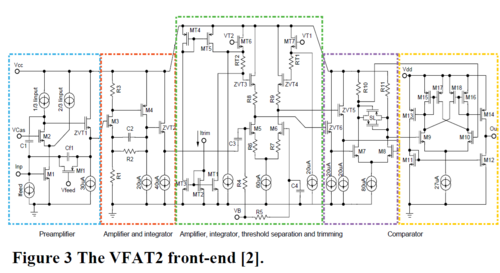
The following is the schematic for the VFAT2 front-end. Some of the VFAT parameters accessable via the I2C can be seen in the schematic. There are still many parameters in the registers that are not found on the schematic and I/Os on the schematic that do not appear to have any representation via the registers.
The current version of the v1495Lib files are completely compiled and loaded onto the ROC. This includes the change made to insert the number of the VFAT chip in place of the header for the ChipID word. I have listed them in text format on the following wiki pages. v1495Lib.c and v1495Lib.h
The CODA gen_list.crl file is found at V1495_CODA_CRL_File
6/25/09
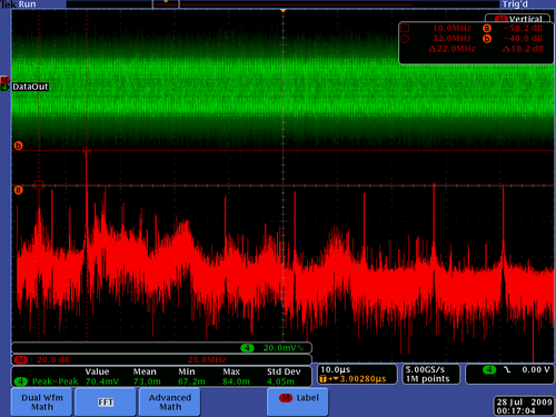
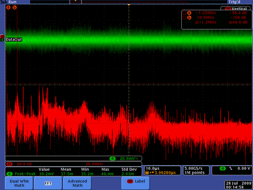
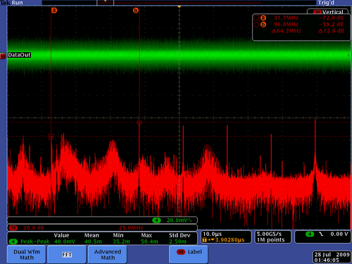
In thinking about the noise on the GEM Trigger line I took the following scope picture of the FFT of the GEM trigger line.
(I can't post it yet because the wiki won't let me.)
We can see from this that there is a signification amount of noise being injected on the GEMTrigger line from the MCLK not only at its fundamental frequency but its harmonics.
Warren, check out the "vfat" executable program in my directory on the DAQ computer.
It will dislay the hits in all 6 VFAT cards graphically
type "vfat -pause -GUI" to see it work
remember the default input file is temp.dat
6/26/09
After having flipped the MSPOLARITY bit, I have observed that we are still getting a significant number of hits in the VFATs. I'm not 100% convinced that we don't have the voltage on the GEM detector cranked up too high and that we aren't observing ringing in the lines one way or the other. We need to do a little more background research to figure out what is going on in the signal lines for the VFATs. I believe that this includes understanding how the frontend section of the VFAT2 works. Also, it requires a better understanding of the register settings. I also highly recommend we get the VCAL functionality of these chips working and hit the lines with some test voltages to see what happens. I think that I could have this part working within a couple of days next week.
I spend the good portion of the day trying to figure out the circuit schematic from the VFAT2 paper that I found online in the CERN document library. I have highlighted the different sections with colored boxes.
Anyway, the first section (blue) is the transimpedance (i.e. current-to-voltage) conversion section. I'm still a little fuzzy on exactly how this section works, however it appears that Ifeed controls the amplification via a cascode amplifier and Ifeed in conjunction with Vfeed controls the high-pass properties of this section. Again, I'm not 100% certain, but it appears that the higher the difference between the biasing voltage set by Ifeed and the value given to Vfeed, the faster this section will sink the negative charge from the line (i.e. the high-pass filter will have a higher cutoff frequency). This section inverts the polarity of the signal. As of yet, I am still uncertain exactly how these parameters correlate to the parameters that are programmable via the I2C registers of the VFAT.
The second section (red) is another amplifier only this time the negative feedback loop sets the low-pass filter properties. Again, I am not certain how the parameters of this section correlate to the programmable registers of the I2C. My guess is that the current sources in this section on the schematic are related to the parameters IShaper/IShaperFeed. This section again inverts the signal.
The next section (green) is where the threshold voltage settings take effect. Setting VThresh_2, _1 set the biasing points of the two sides of the differential amplifier. C3 capacitively couples the signal from the previous section to this section possibly providing even more low-pass filtering on the signal; depending on the frequency of the signal, value of this capacitance, and the magnitude of the current source from the previous stage. The current source Itrim is most likely the parameter that is altered by the individual channel TrimDAC settings. This setting would help balance the imperfections in the different channels' capacitances as well as the imperfections of the various transistors and resistance values. This section inverts the signal as well as converting it from a single-ended signal to a differential one.
It appears that if Vthreshold_2 > Vthreshold_1 then the tripping threshold will be positive; the greater the difference between the two, the higher the positive tripvoltage will be. If Vthreshold_1 > Vthreshold 2 then the tripping voltage will be negative. For either case, if Vin < Vtrip then the output will be a low (logic 0). If Vin > Vtrip then the output will be a high (logic 1). This makes sense for the positive trip voltage but it is opposite of what I thought for the negative tripping voltage. I believe this is whether the MSPOLARITY bit can be used to flip the logical output of the threshold comparator. I would guess that we have been incorrectly making measurements. Using the calibration pulses will most likely help us determine this.
The comparator section actually has two different sections. The first one (purple) converts the different threshold signal to a AC-coupled digital comparison, the two possible values being a function primarily of the value of the current source and the resistor values.
The second section of the comparator (orange) converts the AC-coupled, digital comparator signal into a DC, digital comparator signal with its voltage now being between the high and low values of the DC voltage supply. Once again, I am not certain how the parameter IComp works with this section. If I had to guess, I would say that this only controls the analogue side of the comparator by swinging the biasing point of this section as well as the bistable values of the output.
One thing that is interesting to note about the comparator section is that this is no indication of how the MSPOLARITY bit in ContReg<0> works. The overall polarity of the comparator in the schematic is the same as that which is coming in. Therefore, it is impossible to tell from this circuit how changing the MSPOLARITY bit has affected the results of our experiment. Ultimately, I believe that we are probably going to have to send some calibration pulses down the lines to determine if all of our polarities are correct.
Let's do the detector off test.  I'll lower Vdrift to equal Vgem.
This will keep the GEM amps on but turn off the drift.
Then lets see what hits we get.
We will increase threshold until they go away.
6/29/09
I have successfully been able to write a program, "CalChannels.arm," that will change the CalChan bits for the Even, Odd, or All Channels. To change which of these one uses simply add the option at the end of the program name, e.g. -even, -odd, -on, or -off. The names should speak for themselves at to their functionality. (Right now it only alters the first six channels since that is all one can see on the website.)
I have attempted to use the calibration settings to determine the polarity of the pulses as well as the order of the bits in the data package, but to no avail. I am still a little unclear as to how this works exactly. At first I was trying to use the CalPulse to give me hits I could read out of the VFAT data package, but then I realized that since there was a time delay from sending the CalPulse signal to sending the LV1A pulse on the T1 line, I will probably not be able to use this method unless I set the latency correctly. This may still be an option, although it may take some v1495 firmware tweaking as well since I'm thinking that I may have to send the CalPulse signal immediately before the L1VA signal.
I then tried to send the CalPulse and look at the HitCount register to see if I got a hit or not, but I'm still not exactly sure how the HitCount register is responding to this. I was able to change the value in the HitCount register, but it did not seem to correlate to the Trigger pulses that I was sending. Also, the VFATs do not respond well to single shots of 32Mhz. I tried slowing the MCLK down again to 10kHz, but this did not seem to solve anything.
6/30/09
The following are the questions for Paul Aspel and/or Walt(er?) Snoeys:
The first is a generic question is whether or not there are more reference materials than what we already have (i.e. the VFAT2 Operating Manual and the p292.pdf from the CERN document center). Whether that material would be useful or not most likely depends on whether it addresses the following questions. Of course some of these question might also be answered via a phone call.
What are the relationships between the registers that can be programmed via the I2C, e.g. primary registers 0-9 and extended registers 129-132, and the voltage and current references shown in the front-end schematic of the p292.pdf document? I can somewhat surmise the correlation, but one can see from my previous discussions that there are still too many unanswered questions. Also, can we safely say that this schematic even actually represents the actual circuit used in the design. It seems like there are a lot of missing sections, e.g. how the CalPolarity and MSPolarity bits actually shift things.
Is there more information on exactly how the hit registers work? Where is this information stored in the chip? How do they get set and reset? In particular, if I'm sending a calibration pulse to the channels, shouldn't I see this getting registered as a single hit in the hit counters? (This is with the setup of having HitCountSel<X> all set to zero for fast ORing of the channels, the MSPulseLength<X> set to zero for a one period, and assuming that the VCal is higher than the VThreshold settings.) Also, is there more information on how the calibration timing works and whether it is possible to use the calibration pulse to generate hits on the VFAT2? It would be nice to be able to send a calibration pulse to the outputs and observe these lines getting hits when we call a LV1A command on the T1 line.
Is there a much more detailed discussion somewhere are all of the bit settings in the Control Registers 0,1? I have a lot of questions about these; particularly the most of the MSBs in these registers.
Also, I was wondering if we could find out exactly what algorithm they are using for the CRC on the end of the data package. It claims to be CRC-16, but my efforts to reproduce these checksums using CRC-16 so far have been thwarted.
7/1/09
Although it does not state in the Quartus II help files what the range of acceptable input frequencies is, one is able to get the following error message if too low of a frequency is selected.
Error: Can't implement clock multiplication and clock division parameter values for PLL
     "|v1495usr|GEMReadout:I0|PLLBlock:PLL_0|altpll:altpll_component|pll"
Error: inclk0 input frequency of 0.01 MHz for  PLL
     "GEMReadout:I0|PLLBlock:PLL_0|altpll:altpll_component|pll" must be in the frequency range
     of 15.0 MHz to 1000.0 MHz
Therefore, we should probably have two different versions of the firmware: one with the PLL for a target speed of 32Mhz and one without the PLL for a target speeds less than 15Mhz. If we even need to run the v1495 at a speed other than 32Mhz but still higher than 15Mhz, we will have to recompile the firmware with the correct targeted value.
- I'm going to attempt to start writing sections of my thesis today. (I have a feeling that my first attempt will be someone inadequate.)
From the following two pictures I found in the VFAT annals, we can see that the bit order of the channels in the data packet is from the highest down to the lowest channel number. As for figuring out which lines on the GEM detector physically connect to which inputs we need to observe how the lines get routed from the Kapton sheet to the connector. From the connector to the VFAT one can tell by looking in the VFAT manual and subsequently observing the VFAT ASIC and its board where the signals are routed.
ENC = "Equivalent Noise Charge"
The following paper discusses the usage of this term with some simplified noise circuits.
7/2/09
In attempting to figure out exactly how the MCLK works on the VFAT, I finally figured out that not only is MCLK the VFAT synchoronous clock but that the S<1:8> pins are the regional hit trigger output pins that are programmable via the TrigMode<1:0> bits in ContReg<0>. Right now we don't have any connections to these pins so we cannot use them as regional triggers.
I am attempting to reconstruct the CalPulse experiment in order to figure out if our parameters are set correctly. Right now the settings for this experiment are as follows:
MCLK = 40Mhz

CalMode<1:0> = 0x1 //sets CalOut to VCal
CalPolarity = 1 // makes CalOut pulse negative
MSPolarity = 1 // hopefully makes a "hit" 1 and a "miss" 0 going into MS O/P
TrigMode<2:0> = 0x0 // doesn't matter since we aren't using S<1:8>

ReHitCt<1:0> = 0x //
LVDSPowerSave = 0 // not interested in saving power at this time
ProbeMode = 0 // don't know what this does -- left it at default
DACSel<3:0> = 0x0 // puts DACo-V/I in normal running mode

IPreampIn 0xA8
IPreampFeed 0x50
IPreampOut 0x96
IShaper 0x96
IShaperFeed 0x64
IComp 0x78
MSPulseLength<2:0> = 0x0 // MonoStable pulse length of 1 clock period
HitCountSel<3:0> = 0x0 // Fast-OR of all 128 channels
Lat 0x00
VCal 0xff     // VThreshold intentionally set much lower than VCal
VThreshold1 0x10
VThreshold2 0x00
CalPhase 0x00 // don't know how this works exactly -- thus, turned it off
The MCLK frequency was chosen because it is the original Calibration pulse frequency at which experiments were run. Also, in the experiment the CalPulse signal supposedly has a peaking time of ~22ns. Thus, if we want to have any hope of catching the calibration pulse, we will most likely need to run at at least 40 Mhz. This, of course, also depends on the peak amplitude of the pulse as well as how long its tail is.
The v1495 firmware performs a straight pass-through of the trigger signal from the pattern generator. Care has been taken to make sure that the signals are passed along while they are stable rather than at a transition. Also, it is known that the MCLK shown in Figure 10 of the VFAT manual is out of phase by 180o; thus care has also been taken to make sure that the T1 signal has the proper phase with respect to MCLK. This whole process causes the signal being output to be one clock cycle behind the signal being injected; this shouldn't be a problem.
On our Agilent pulse generator, the "TRIGGER OUT" channel is used as the MCLK for the VFATs and "OUTPUT1" as the T1 signal for the VFAT. OUTPUT1 is set such that it will output the Calpulse signal followed by a single break pulse and then followed by the LV1A signal. The pattern is long enough that we should be able to see whether we received any hits on the lines that we have CalChan turned on in the respective ChanReg. Right now the experiment is running too quickly and does not have the proper setup to see whether the HitCount registers are working properly with the calibration pulses being sent.
I'm also hoping that I might be able to gate the signal from the pattern generator so that I will be able to use the HitCounter.
The following picture shows a "CalPulse" signal with one clock cycle break followed by an LV1A pulse. I am still unable to get any hits in any of the channels from this.
7/3/09
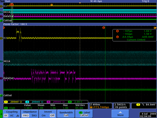
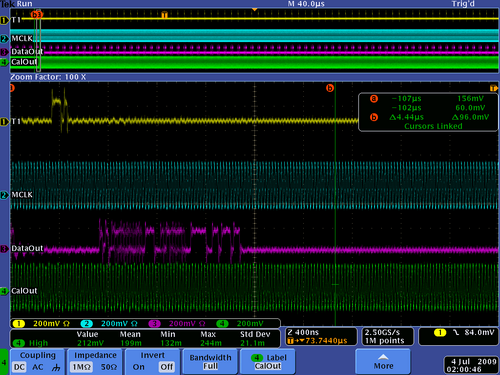
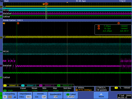
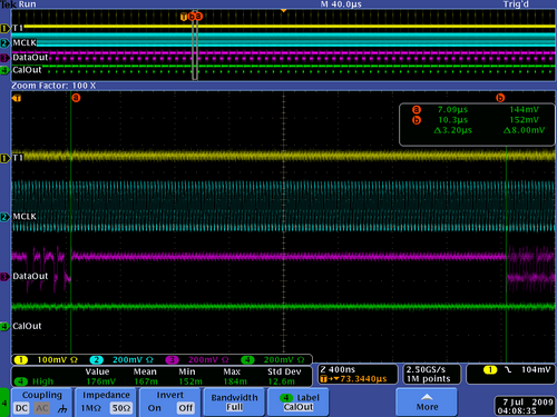
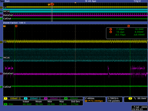
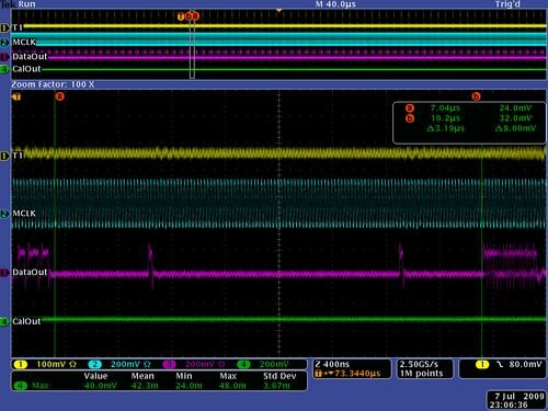
The following demonstrates my attempts to analyze the VCal and CalOut signal externally. There is some noise from the clock (40Mhz) injected onto the DACo-V line due to the two lines partially running parallel to each other on the board.
The following pictures were taken to measure the VCal voltage both when the register was set to its highest value (lowest voltage) and lowest value (highest voltage) respectively. Delta V is about the same here as purported by the data sheet of ~200mV, but the absolute values are off by almost half of a Volt. I could be wrong, but I believe that the scope I'm using has a floating ground for the probe. Besides that we have a hefty grounding strap between the scope and the board, so this shouldn't be a big issue. It would have also been nice to measure the baseline voltage (which I believe is a bandgap voltage source) on DACo-V, but I do not see this capability.
One can see it, but I will explicitly note that the fourth line is the measured signal of interest with the scope set to an input impedance of 1MOhm. Also, the scale was changed from 2V in the first pictures to 200mV in the second picture. That is why the clock noise appears so much larger.
DACSel<3:0> = 0x9 and CalMode<1:0> = 0x1.
The following picture was taken in an attempt to view CalOut while connected to VCal. I would have expected there to be no change between this and the last picture, but as one can see, the signal appears to be grounded for some reason. For this picture in particular, I was expecting a positive pulse on the CalOut signal after the CalPulse command on the T1 line.
For this picture DACSel<3:0> = 0xB.
7/6/09
After having talked to the design engineer, Paul Aspell, we were able to figure out a couple of problems with the CalPulse experiment: first of all, I should have realized that hooking ~13pF probes in parallel with this sensitive charge circuit would most likely destroy any trace of the charge pulse that is being generated on the CalOut node; second, and perhaps the most crucial is that one cannot have the DCUout connected with the CalOut node while trying to perform this experiment. I was assuming that the DCUout was sufficiently buffered from the CalOut node. One needs to completely open this connection by unsetting CalMode<1:0>. (The DACsel<3:0> bits do not appear to alter the performance of this test.)
The following pictures were taken of the outputs from the VFAT. The payload bits are in between the green cursors. These pictures were taken with VCal = 0xFF, Vthresh1 = 0x0, Vthresh2 = 0xC, CalPol = 0, MSPol = 0, and MSPulseLength<2:0> = 0x7. (I found that even at 40 Mhz the first pulse was too quick even if the LV1A signal immediately followed the CalPulse signal. Therefore I extended it out a bit. Also, the threshold I used for Vthresh2 was the smallest threshold that I found would completely suppress any spurious hits on the channels.
This picture shows all of the channels turned off.
This picture shows all of the channels turned on.
This picture shows all of the odd channels turned on.
This picture shows all of the even channels turned on.
Furthermore, I found that when I flipped the polarities of Vthresh1 and Vthresh2 and then changed CalPolarity, MSPolarity = 1 that I was able to duplicate these results the other way.
- I am still not able to directly measure the DC CalOut signal as I feared even after the discussion we had with Paul this morning; I even tried flipping the CalMode bits back and forth since the settings for CalOut to VCal/Baseline are backwards in the old manual vs. the newer one. I will not be able to do a proper Qinc vs. VCal graph without this. I can do one with VCal hooked up directly to DACoV, but this will have an offset (and possibly other factors as well) due to this being the VCal signal before it goes through an amplifier.
7/7/09
The following two pictures were taken with a negative CalPulse (i.e. Calpolarity, MSPolarity = 1). The first picture is of Channel 25, the second picture is of both Channel 25 and Channel 100.
- Suppressing the noise on the GEM lines still results in us not being able to send in a readable CalPulse. I won't be able to do an S-curve of the VFAT channels while hooked up to the detector until we get this fixed. I even tried slowing the clock down to 500kHz to see if the MCLK wasn't the primary noise source, but this still did not work. I tried to manipulate several of the Preamp-type settings to see if I could get a better reading but was unsuccessful. We just need to know what these settings do exactly in order to get them to work.
The most pressing questions I have for Paul Aspell:
How do the HitRegisters work? (This includes how ReHitCT<1:0> work.)
Why can we not measure the VCal signal through CalOut when CalOut is hooked up to DACoV?
How do the Preamp settings work? Is there a diagram somewhere to explain these better? (Primary registers 2-7.)
How do the TrimDAC<4:0> work?
7/8/09
After our discussion with Paul this morning, we were able to confirm that we were indeed doing this setup at least theoretically correctly; I had the apiphany -- due to all of the other typos in the older VFAT manual -- that maybe there was still a typo in our manual. Indeed, if one counts the hex numbers for the different configurations of DACsel<3:0> one will notice that 0xA is missing. I attempted this instead of 0xB in order to read CalOut, and it works. I have listed the measurements from the different nodes below:
| For VFAT16: | |
|---|---|
| VCal "high" | 1.37 V |
| VCal "low" | 1.16 V |
| Vthreshold1 "high" | 2.16 V |
| Vthreshold1 "low" | 1.14 V |
| Vthreshold2 "high" | 2.16 V |
| Vthreshold2 "low" | 1.22 V |
| Baseline | 1.36 V |
| For VFAT32: | |
|---|---|
| VCal "high" | 1.38 V |
| VCal "low" | 1.18 V |
| Vthreshold1 "high" | 2.15 V |
| Vthreshold1 "low" | 1.22 V |
| Vthreshold2 "high" | 2.15 V |
| Vthreshold2 "low" | 1.21 V |
| Baseline | 1.37 V |
I still wondering what the best way is going to be to set this up so that we can plot our S-curve results. It seems to me -- the longer I think about it -- that this is probably the time to figure out how, when, where, and why we are going to trigger the v1494 as well as the SIS3600. There was still a little bit of room for improvement there for sure.
For instance, I have a couple of questions that need to be answered before I proceed, because it may be best to answer them now so that we do not need to implement any major changes to our programs in the future.
We had talked about having the CODA query the v1495 at approximately 1kHz. A LV1A trigger can be as quick as 3 MCLK cycles and the VFAT can remember 1024 LV1A requests (if I'm not mistaken); so as long as we don't outrun this capability of the VFAT, we should be okay. Running the MCLK at a speed lower than 1GHz gives us 2-3 readouts of the data packet before the system would probably have to pause to let the CODA read the results. Right now while we are taking data the cosmic triggers are on average much slower than that, however, when we were taking data before, if more than one trigger came within a second of each other, the subsequent events were being ignored within that second time period. For the purposes of the S-curve and for the future we should plan on catching all of these events.
In order to do this I'm thinking that a small tweak of the v1495 firmware is going to be in order. I may need to send a more complicated "word" than the HARD_TRIG_WORD or the SOFT_TRIG_WORD based on a given input pulse. I am thinking that the v1495 will need to keep track of how many events are left in the EventDataFIFO and report a trigger for the CODA to take the data from the ROC at the appropriate times.
7/10/09
the M4K blocks in the Cyclone devices should be able to perform true dual-port functionality, i.e. they can read and write at the same time to different addresses. Due to this fact, it is probably even less important to implement any kind of readout control for the SIS3600 from the v1495.
Having reviewed the way the I/Os are setup on the v1495, I have found it to be impossible to set the two different G ports to different I/O directions (or voltage levels for that matter). Thus, I won't be able to impliment the idea that I had of having the G1 port output the trigger to tell the SIS3600 to read the VFAT data packet. We could purchase another LEMO I/O module to give us this capability, but I'm thinking that the benfits from the increase in speed that we would see would probably not surpass the cost of purchasing the module; particularly since other universities would have to have this extra module as well to have this functionality. It is just simplier to send a separate delayed pulse to the SIS3600 to instigate a v1495 read.
While updating the firmware to perform the calibration sequence I found a critical error in the way the software reset was being implemented. Basically the reset was running in sync with the LCLK rather than the PLLCLK. If the PLLCLK was running at or near the LCLK then it probably wouldn't have been a problem. However, if we were to reduce the speed of the MCLK, we would have about a 100:1 chance that we would not get the proper reset. I'm really glad I caught this. This may also explain several issues I was having earlier.
7/12/09
The reset functionality is finally working the way it should have been the whole time. Now when one sends a reset signal to the v1495 it truly resets everything including the VFATs. I can send a single CalPulse/LV1A sequence now by writing to register 8 on the v1495. In the future, the word that you write to that register will be how many time the CalPulse/LV1A signal gets repeated.
I was not able to setup the cosmic thresholds yet. I will do it first thing in the morning on Monday; I'm hoping Brian's work on the Gumstix does not interfere with this, but it seems like that's a pretty high priority project for this week as well.
7/13/09
I fixed port 48 on the breakout board. There were some GND and VCC connections that weren't very good. They might have been bumped loose in the process of moving the board around. The new solders are much stronger, so hopefully we won't have that problem again on this board.
7/15/09
I found out how to use the functionality already included in the vfat program for the CODA to output to a text file. The problem I was having before was apparently when the TApplication class object is instantiated, if the output file already exists then it strips it out of the number of arguments on the command line. One could conceivably alter the code to not do this, but the easier thing to do is to just enter in a non-existent file each time.
Now that I know this -- along with my Calibration functionality I added to the v1495 -- creating S-curves should be rather uncomplicated. I would like to wait until we have the new board working though to do this. That way we will see the S-curves for the noise levels on the working boards.
7/23/09
I have verified that all of the VFAT ports are working with the exception of Port 80 and 112. DataValid on Port 80 appears to be having issues for some reason. I can't test Port 112 until we can update the flipbit code to allow access to this address. It doesn't really matter too much since we only have four working VFAT cards right now anyway.
I have also updated the VFAT.setup script so that it doesn't mess with the I2C expander. I had to figure that out because the old VFAT.setup script was soft resetting two of the VFATs. I still don't know how the other card expander works exactly. I'm sure I'll be able to more easily figure it out once Brian gets Cairo so that we can cross-compile programs and I can get a hold of some of his source code.
7/24/09
Port 80 on our breakout board is still not working properly. I can see a DFTestPattern as well as a DataValid pulse coming out of this, but it is unresponsive to a LV1A request. I have checked every pertainent connection that I can think off to fix this problem. It is definitely a problem with the port as one can use the same VFAT on different ports successfully, and one can use a different VFAT on this same port and have the same problem.
It is therefore probably going to be more efficient to get a new board up and running to see if the same problem persists.
I still can't test Port 112 because we cannot cross-compile the new code for the new Gumstix yet.
Tamuna and I tried to get the GEM detector working but after even just plugging in the board, we get more noise than the height of our signal. This was without even turning on the pulse generator with the MCLK. This really made the noise very high. Why would just plugging the VFATs into GEM detector cause so much noise? That doesn't seem to make much sense as of yet.
I recommend we heavily investigate how to mitigate our SNR problems. The first and most obvious thing we can do is some kind of notch filter at our MLCK frequencies and their subsequent harmonics or maybe a band-pass filter depending on how we want to tackle the problem. The problem with the notch filter is that it will be frequency specific, but that may be the price we have to pay to kill out the MCLK noise.
Another way we could try to tackle this problem is to improve the signal coming from the GEM detector. We could possibly come up with a better design of the HV distribution network that would give us better results.
Obviously with all of these ideas there is the looming issue of radiation hardness of the components we use. As of this time it is not something that I personally am all that familiar with, but it may be worth the time and effort to do some research into what kind of circuitry we can in fact use on this board.
I set the following thresholds
V16 = 0xdd
V48 = 0xf1
V64 = 0xda
V96 = V1495 output for this VFAT board was always high so I unplugged the VFAT
Began run 1172 with coincidence between 2 PMTs
ET crashed. Theory is that the V1495 injected more data than expected overfilling ET buffer.
interrupt: ERROR: v1495ReadEvent returned 0 words
perhaps we should reset the V1495 after the above error message
7/25/09
16 = 0xf1
V48 = 0xfa
V64 = 0xfc
V96 = V1495 output for this VFAT board was always high so I unplugged the VFAT
Began run 1173 with coincidence between 2 PMTs
GEM HV = 3500:3200 Volts
7/27/09
The following two pictures were taken at the breadboard level on the power supply for the VFATs. The channel (green) is AC coupled to show only the AC ripple in the signal. The FFT of this signal is in red. The cursors are also shown in these pictures for comparison. Four VFATs were running while these pictures were taken. More than likely this data does not represent the noise when the VFATs are delivering a data packet. We may need to capture a picture of this separately as this may show even higher noise.
The following picture was taken with the 32Mhz clock on.
The following picture was taken with the 32Mhz clock off.
In the first picture we can see significant noise due to the clock at its fundamental frequency and higher order harmonics. The second picture shows that we still have a significant amount of noise below 225Mhz even with the clock turned off.
The elimination of the noise in the power supply presents a bit of a technological challenge. My previous experience is with eliminating noise from the power supply itself. While we most likely do in fact have noise coming from the power supply, we are also seeing the introduction of noise from the clock lines themselves. It's as if we need to deaden the ability of the power supply to see this induced noise at the site, i.e. we need to make it "harder" for the clock to induce a voltage in the power supply by creating a filter that will dump that excess energy to ground. We also need to create a filter on the power supply side that will give us a more consistent DC voltage. I'm not 100% sure how to accomplish this yet.
The following picture was taken of the output with a 100uF bypass capacitor at the supply site. The clock was still on in this picture. We can see that the noise from the first harmonic of the clock signal is greatly reduced in magnitude although the content from some other harmonics are still very prevalent.
I would be curious to see whether the introduction of this extra capacitor has any effect on the noise seen by the GEM Trigger. If it does then we may have a bigger output impedance problem on the power supply than originally thought.
V1495 crashes ET
below are the log messages leading up to the ET crash
interrupt: v1495DataReady return 1 words
interrupt: v1495FillData return 84 Buffwords
interrupt: v1495ReadEvent: Error: header for word 3 from data packet != 0xE
interrupt: v1495DataReady return 1 words
interrupt: v1495FillData return -1 Buffwords
interrupt: v1495ReadEvent: Error: header for word 3 from data packet != 0xE
interrupt: v1495DataReady return 1 words
interrupt: v1495FillData return -1 Buffwords
interrupt: v1495ReadEvent: Error: header for word 3 from data packet != 0xE
interrupt: v1495DataReady return 2 words
interrupt: v1495FillData return -1 Buffwords
interrupt: v1495ReadEvent: Error: header for word 3 from data packet != 0xE
interrupt: v1495DataReady return 2 words
interrupt: v1495FillData return -1 Buffwords
ERROR; write_thread failed (in recv).
rolp->daproc = 3
We need to find out why BuffWords is empty as this is used to increment the buffer pointer.
For now I put an if statement in the readout list CRL file.
The following check in the CRL file solved the ET crashing problem
	if(BuffWords>0){
	  rol->dabufp += BuffWords;
	}
	else{
          v1495Reset(); /* The VFATs sometimes do not sent data to V1495 */
         }
7/28/09
I was able to assemble a new board. All of the ports including Port 80 and port 96 appear to be working, but when I was sending a Reset Pulse to these two ports they would send a data packet, and when I would send a CalPulse they would not respond. I'm not quite sure why yet.
It also appears that the v1495StatusPrint() function got changed and now it is really difficult to use for debugging.
After more testing of our noise problem I was able to filter out the noise on the board, but found ~14Mhz noise on the line (I'm thinking that this is coming from the Gumstix). I think that our pulse generator is creating noise on the line. I did some research and found some line conditioners from TrippLite that can isolate equipment within the same power strip.
7/29/09
We were able to order a line conditioning unit from Tripp Lite.
8/3/09
I've been able to expand the written explanation of the firmware.
How much do I need to include on the sections of code that were written by someone else: for instance, how much do I need to explain from the firmware update code? Do I need to thoroughly describe this section?
 The entire code will appear in an Appendix.  There should be a block diagram
in the main text which outlines the functionality of the code.  The places another
person would need to edit the code are the key points which need a lot of explanation.
How do I change the output channel logic so I can see a copy of the DATout signal or
generate a LV1A pulse for calibration, ...
I think I may have located part of the problem as to why we aren't getting some VFATs to deliver data packets. This may also explain why some VFATs give a data packet when a ReSync signal is sent to them as well. The picture below shows the extreme ripple in the Trigger line on Port 16. There is only supposed to be one pulse there. For some as-of-yet inexplicable reason we are getting ripple in the trigger lines which look like multiple pulses. This would look like a BC0 signal to the VFAT which does not tell it to send a packet which is why there is nothing on line 3 (DataOut) in the picture.
I am not sure what is causing this, but it is definitely a problem.
it looks like reflections from termination cable mismatch (wrong termination; no 50 Ohm symbol showing on Channel 4 label)
Added 8/4/09

The fact that there is no 50-Ohm termination on the cable was done intentionally. I inserted the scope in parallel with the VFAT
LVDS receiver for the Trigger signal. In theory this should only add the differential impedance of the scope in parallel to the
impedance of the receiver (e.g. a very large impedance). However, I believe you are correct that this looks awfully reminiscent of
reflections.

I'm wondering now if by adding extra common-mode capacitance to the LVDS lines on our new breakout board by running them over the
power planes that we haven't inadvertently added an excessive amount of differential capacitance. Furthermore, this capacitance may
be greater than what the LVDS signals can handle and hence causing our reflections. However, right now it doesn't make sense to me
how we could have added differential capacitance to the signal by doing this.

If we can run at a much lower speed and/or if we run at this speed on the old breakout board we may be able to determine if this is
the problem and what the potential fixes may be.
It is possible that it can be cured by running at a much slower speed. It may due to having a new V1495 or a new cable or a combination of the two. I definitely remember never seeing anything like this before. I also tried to unplug the VME crate from our new power line filter, but this had no appreciable effect either way. Even when I measured the signal coming straight from the V1495 I was getting a really terrible output pulse which kind of rules out our new boards being the problem.
I'm going to try to switch cables tomorrow, but I doubt this will fix the problem. I am also going to try running at a much slower speed. I will have to think some more on what could be causing this and what else if anything can be done about it.
8/4/09
In trying to determine why certain ports are and are not working, I've discovered the following similarities and differences.
The trigger signal of which I took a scope picture yesterday is the only trigger line that runs over analog ground. This may be the source of capacitive coupling that we are seeing for this signal.
Ports 80, 96, and 112 all have their Trigger lines running for a short distance through the digital ground plane. These connections appear to be connected properly while doing a continuity test, so I don't believe that this is the problem. To do this I ran a VFAT cable between ports and measured the resistance between similar pins, i.e. MCLK to MCLK or Trig to Trig. I also checked to make sure that they were not shorting to the other planes, and they were not.
These connections could still be the source of the extra capacitance that may be the cause of transmission reflections. In the sections where they run through the digital ground plane this could be particularly true since they will be strongly coupled to both the ground plane and the VDD plane. If this is the case, then port 112 will most likely not work either. This is at least a testable theory. I think that I might have been foolish and due to convenience only tested whether the trigger signal was making it up to the via before the signal goes down to the analog ground plane. Previously I had not noticed that these signal were doing this. I will disconnect the VFATs and test at the pins whether or not this trigger signal is making it to the pins.
I think I've convinced myself where the differential capacitance comes from in this configuration. In an effort to increase the common-mode capacitance (particularly between wires) we've effectively bend the field lines towards the power planes. At first glance it should appear that this does not effect the differential capacitance between the two because the net effect should be negated between the two. However, if one decreases the strength of the field lines between two conductors with the same charge then by the definition of potential the voltage will decrease between the two and by the definition of capacitance the capacitance between the two is increased.
On a slightly different note, I found the following discussion from a National Instruments manual on LVDS to be interesting and possibly something else to watch out for with LVDS signals.
COMMON MODE RANGE
An LVDS receiver can tolerate a minimum of ±1V ground
shift between the driver’s ground and the receiver’s ground.
Note that LVDS has a typical driver offset voltage of +1.2V,
and the summation of ground shifting, driver offset voltage
and any longitudinally coupled noise is the common mode
voltage seen on the receiver input pins with respect to the receiver
ground. The common mode range of the receiver is
+0.2V to +2.2V, and the recommended receiver input voltage
range is from ground to +2.4V. For example, if a driver has a
VOH of 1.4V and a VOL of 1.0V (with respect to the driver
ground), and a +1V ground shift is present (driver ground
+1V higher than receiver ground), this will become +2.4V
(1.4+1.0) as VIH and +2.0V (1.0+1.0) as VIL on the receiver
inputs referenced to the receiver ground (+2.2V VCM). Similarly,
with a −1V ground shift and the same driver levels results
as 0.4V (1.4−1.0) VIH and 0.0V (1.0−1.0) VIL on the receiver
inputs (+0.2V VCM). This is shown graphically in
Figure 3.
Tomorrow I will compare the reflections on the other ports to determine if this is indeed the reason for all of our mysterious behavior on our new breakout board. I will also test everything on the old board at the same speed to see if getting rid of the ground planes will mitigate the differential capacitance.
One solution to our problem would be to add some kind of filtering on a new breakout board that compensates for the increase in differential capacitance, i.e. RF surface inductors.
Another solution to eliminate cross-talk between wires (in the event that we get rid of the ground planes and the cross-talk becomes too much) is to run the clocks for the different VFATs alternating 180 degrees out of phase with each other. This would require a more sophisticated capturing scheme in the V1495 itself, but it is at least an option to explore in given the events as described. (Half of the VFATs would have their data captured on the rising edge of PLLCLK_90 instead of PLLCLK.)
8/5/09
The following shows the ripple in the power planes on the new breakout board.
The following pictures were taken of the T1 signals on the new breakout board.
I slowed down the speed from 32Mhz down to 500kHz and it appears that the first four port now work. Interestingly enough, when I sped up the speed to 40Mhz or enough 60Mhz, some of the VFATs were still working. It appears that from about 30Mhz-38Mhz the first four ports do not want to work. That's just the first four ports.
The last two ports do something else different. The last two ports (e.g. port 96 and port 112) do not work at any speed by themselves. At 500khz if I insert the scope probe at 1MOhm they start working intermittently. If I insert a 1MOhm resistor and then put my finger across the resistor they start working normally. I would guess that this action of putting my finger across the resistor is the same as adding some resistance in parallel differentially as well as a minute amount of capacitance differentially. It would also be adding some very large resistance to ground single-ended as well as some large capacitance to ground single-ended. If I try to stick in just a resistor (1MOhm or 470kOhm) and/or a capacitor (10uF), it does not have the same effect.
8/7/09
I almost have the new board done. I've updated the spacing and component layout for the items that weren't working before. It should be a lot better.
I just need to place the new VCC and GND planes and then reroute. The whole process may take a few hours to get just right though.
I'll try to come in over the weekend to polish it off. I'll probably need Brian's help, however, to double-check my work and to get the correct files to the board manufacturer.
8/10/09
I'm to the point that I have all of the power planes connected. I'm routing the signals, but the autorouter feature on this program is not very helpful. It appears from my experiences here and with what Brian is telling me that this could take a little while longer than anticipated. I'm hoping to be done by the end of tomorrow, but I have a lot of wires to figure out how to squeeze in.
9/2/09
I finished soldiering up one of the new boards, but as soon as I did I found that there was a short between AVCC and AGND. I cannot explain this. I checked the other boards, and they are open. This means that somehow I've soldiered the two short, and I can't see it. I'm tempted to hook it up to a significant power supply and roast the short open wherever it may be. I can't see another way around this unless we have some thermal imaging equipment somewhere around campus I can borrow. It may be conceivable to use the gauss meter to try to pin it down as well. I'm not quite sure how that works though.
9/5/09
After carefully considering the different options for resolving the issue as stated in the previous entry, it became clear that hooking up my spare car battery to the circuit would blow the short open nicely, e.g. not too much sustainable voltage and yet still plenty of sustainable current. This is indeed what I did. The picture of where the short was is shown below. (I must apologize, however, for the new black smudge on the table in the lab.)
I have also included a picture of the board before the short was located.
I am not certain, but it appears that there used to be a stringer going from AVCC layer over to that pin, which would appear to be a board manufacturing error since that certainly isn't there on the schematic. I am hopeful that the board can be tested now, although I'm not sure if the VFAT E DACo-I or the VFAT D DACo-V will work on this board given the location of the damaged area. At least the green LED turns on now when power is applied to the board.
Anyway, this appears to have fixed one problem, but when I went to test the I2C the Gumstix wasn't working. I've emailed Brian to see if he can figure out what is wrong with it.
Warren: document the error with an image of the traces in the design to compare with the traces we see on the board. Once we can show the manufacturer their error we can ask for a replacement
9/9/09
Today Brian was able to get the Gumstix up and running again. I was able to query the I2C IC on the board and change the LEDs, but we are still having issues getting the VFATs to respond properly when queried. It doesn't seem to matter it we switch back to the old board either; we are still having the same problem. It would appear that there may still be an issue with the setup of the I2C as compared to when we last had it working properly.
9/22/09
The I2C issue appears to be fixed for the time being. I suggest that we can attribute that to getting the new I2C boards put together. That includes all ports (Port 48 had one address pin incorrectly placed).
We are still missing one VFAT and associated cable. I'm hoping this has just been shuffled under one of the many boxes we've accumulated since we had everything up and running with the Rev. 2 breakout boards.
I have also uploaded the new firmware to account for the changes we did and all of the ports except Port 112 are working, e.g. they are responding to a T1 with an appropriate data packet. I can't seem to do any testing on port 112 quite yet to figure out what is wrong with it. I think we may have the old firmware loaded that doesn't have port 112 as a valid port, but I'll have to confirm this with Brian. This is in and of itself progress because if I recall correctly we couldn't even get ports 96 or 112 working on the old board.
I'll check with Brian to see if we can get the new ./flipbit program in there and get port 112 working. Immediately after that I'll check for the 40Mhz noise levels on the lines. It will be interesting to see if the new configuration of the TRIG and MCLK lines has helped mitigate some of the crosstalk noise through the cables.
The following is a picture of a T1 response from Port 96. All lines are coming from the test ports on Port C of the V1495.
