Difference between revisions of "JLAB PLX LVDS"
Jump to navigation
Jump to search
| Line 14: | Line 14: | ||
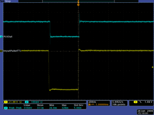
[[Image:PLX_input_and_output_pulses_1.png|300px]] | [[Image:PLX_input_and_output_pulses_1.png|300px]] | ||
| + | |||
| + | |||
| + | =3/17/09= | ||
| + | |||
| + | How to use Input register | ||
[http://wiki.iac.isu.edu/index.php/VME_modules Go back] | [http://wiki.iac.isu.edu/index.php/VME_modules Go back] | ||
[[VME_modules]] Go back | [[VME_modules]] Go back | ||
Revision as of 22:21, 17 March 2009
A VME Modules designed by Ed Jastrzembski at JLAB
Description:
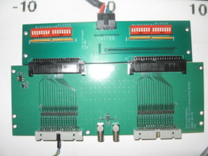
This PLX board will be built on a Flex I/O format that Ed Jastrzembski developed many years ago. The VME (back end) manages the interface to the bus, and controls two front end 'ports' that can be input or output units.
3/17/09
How to use Input register
Go back VME_modules Go back


